Dma write cycles, Dma write cycles –15 – Altera Arria V Hard IP for PCI Express User Manual
Page 237
Chapter 17: Testbench and Design Example
17–15
Test Driver Module
December 2013
Altera Corporation
Arria V Hard IP for PCI Express
User Guide
3. If a suitable BAR is found in the previous step, the driver performs the following
tasks:
■
DMA read—The driver programs the chaining DMA to read data from the
BFM shared memory into the Endpoint memory. The descriptor control fields
(
) are specified so that the chaining DMA completes the following
steps to indicate transfer completion:
a. The chaining DMA writes the
EPLast
bit of the
after finishing the data transfer for the first and last
descriptors.
b. The chaining DMA issues an MSI when the last descriptor has completed.
■
DMA write—The driver programs the chaining DMA to write the data from its
Endpoint memory back to the BFM shared memory. The descriptor control
fields (
) are specified so that the chaining DMA completes the
following steps to indicate transfer completion:
c. The chaining DMA writes the
EPLast
bit of the
after completing the data transfer for the first and last
descriptors.
d. The chaining DMA issues an MSI when the last descriptor has completed.
e. The data written back to BFM is checked against the data that was read from
the BFM.
f. The driver programs the chaining DMA to perform a test that demonstrates
downstream access of the chaining DMA Endpoint memory.
DMA Write Cycles
The procedure
dma_wr_test
used for DMA writes uses the following steps:
1. Configures the BFM shared memory. Configuration is accomplished with three
descriptor tables (
).
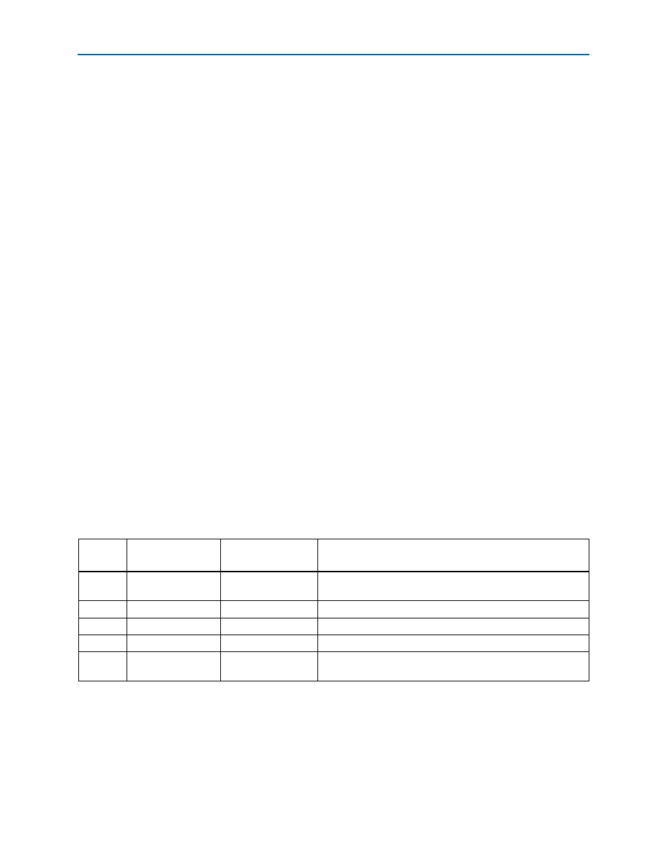
Table 17–11. Write Descriptor 0
Offset in BFM
Shared Memory
Value
Description
DW0
0x810 82
Transfer length in dwords and control bits as described in
DW1
0x814
3
Endpoint address
DW2
0x818
0
BFM shared memory data buffer 0 upper address value
DW3
0x81c
0x1800
BFM shared memory data buffer 1 lower address value
Data
Buffer 0
0x1800
Increment by 1 from
0x1515_0001
Data content in the BFM shared memory from address:
0x01800–0x1840