Table 17–7 – Altera Arria V Hard IP for PCI Express User Manual
Page 235
Chapter 17: Testbench and Design Example
17–13
Chaining DMA Design Examples
December 2013
Altera Corporation
Arria V Hard IP for PCI Express
User Guide
1
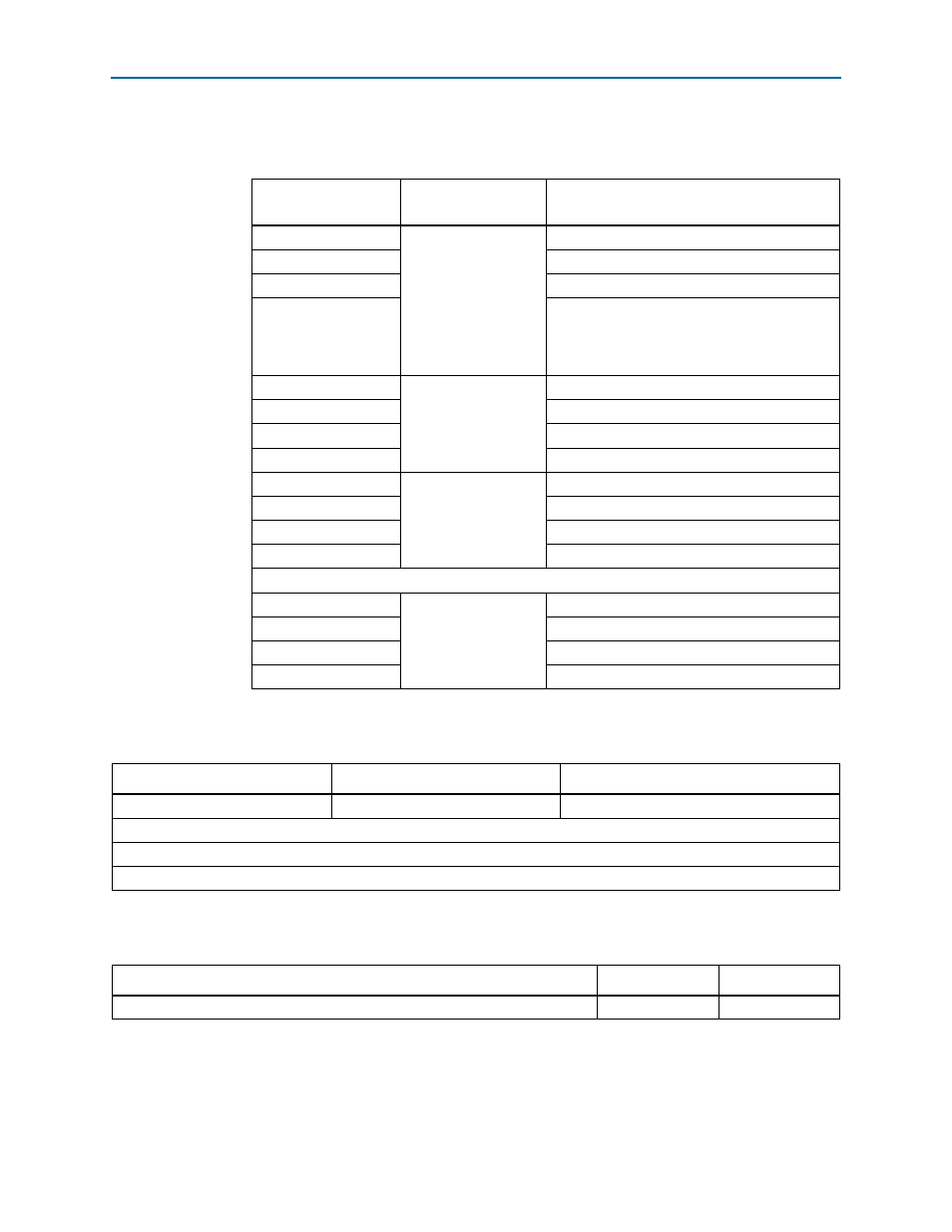
Note that the chaining DMA descriptor table should not cross a 4 KByte boundary.
shows the layout of the descriptor fields following the descriptor header.
shows the layout of the control fields of the chaining DMA descriptor.
Table 17–7. Chaining DMA Descriptor Table
Byte Address Offset to
Base Source
Descriptor Type
Description
0x0
Descriptor Header
Reserved
0x4
Reserved
0x8
Reserved
0xC
EPLAST - when enabled by the
EPLAST_ENA
bit
in the control register or descriptor, this location
records the number of the last descriptor
completed by the chaining DMA module.
0x10
Descriptor 0
Control fields, DMA length
0x14
Endpoint address
0x18
RC address upper dword
0x1C
RC address lower dword
0x20
Descriptor 1
Control fields, DMA length
0x24
Endpoint address
0x28
RC address upper dword
0x2C
RC address lower dword
. . .
0x ..0
Descriptor <n>
Control fields, DMA length
0x ..4
Endpoint address
0x ..8
RC address upper dword
0x ..C
RC address lower dword
Table 17–8. Chaining DMA Descriptor Format Map
3122
21 16
150
Reserved
Control Fields (refer to
DMA Length
Endpoint Address
RC Address Upper DWORD
RC Address Lower DWORD
Table 17–9. Chaining DMA Descriptor Format Map (Control Fields)
2118
17
16
Reserved
EPLAST_ENA
MSI