Table 8–3 on, 0x010, 0x014 – Altera Arria V Hard IP for PCI Express User Manual
Page 156: 0x018, 0x01c, 0x020, 0x024, 0x000, 0x008
8–2
Chapter 8: Register Descriptions
Configuration Space Register Content
Arria V Hard IP for PCI Express
December 2013
Altera Corporation
User Guide
describes the Type 0 Configuration settings.
1
In the following tables, the names of fields that are defined by parameters in the
parameter editor are links to the description of that parameter. These links appear as
green
text.
describes the Type 1 Configuration settings.
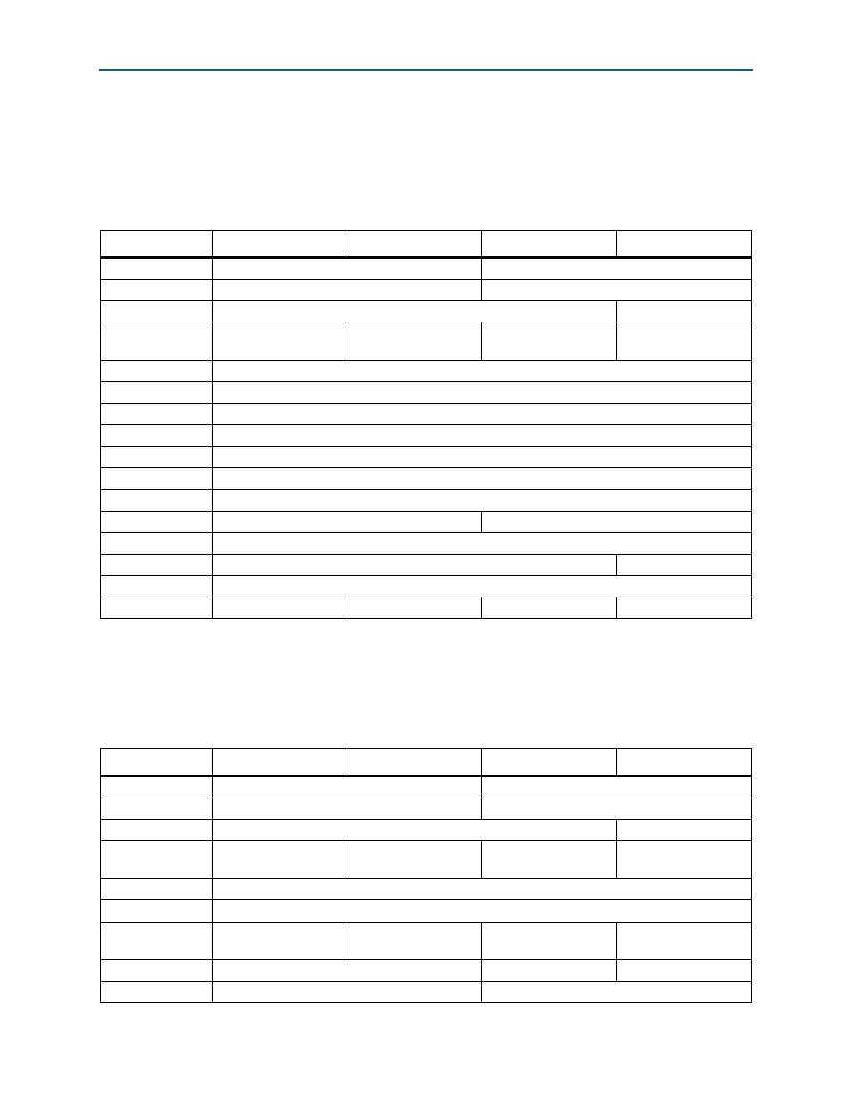
Table 8–2. PCI Type 0 Configuration Space Header (Endpoints), Rev2.1
Byte Offset
31:24
23:16
15:8
7:0
0x000
0x004
Status
Command
0x008
0x00C
0x00
Header Type
(
0x00
Cache Line Size
0x010
Func0–Func7 BARs and Expansion ROM
0x014
Func0–Func7 BARs and Expansion ROM
0x018
Func0–Func7 BARs and Expansion ROM
0x01C
Func0–Func7 BARs and Expansion ROM
0x020
Func0–Func7 BARs and Expansion ROM
0x024
Func0–Func7 BARs and Expansion ROM
0x028
Reserved
0x02C
0x030
Expansion ROM base address
0x034
Reserved
Capabilities Pointer
0x038
Reserved
0x03C
0x00
0x00
Interrupt Pin
Interrupt Line
Note to
(1) Refer to
for a comprehensive list of correspondences between the Configuration Space regist
Table 8–3. PCI Type 1 Configuration Space Header (Root Ports) (Part 1 of 2)
Byte Offset
31:24
23:16
15:8
7:0
0x0000
0x004
Status
Command
0x008
0x00C
BIST
Header Type
Primary Latency
Timer
Cache Line Size
0x010
Reserved
0x014
Reserved
0x018
Secondary Latency
Timer
Subordinate Bus
Number
Secondary Bus
Number
Primary Bus Number
0x01C
Secondary Status
I/O Limit
I/O Base
0x020
Memory Limit
Memory Base