Root port design example, Root port design example –18, Er to – Altera Arria V Hard IP for PCI Express User Manual
Page 240: Root port design example” on
17–18
Chapter 17: Testbench and Design Example
Root Port Design Example
Arria V Hard IP for PCI Express
December 2013
Altera Corporation
User Guide
2. Sets up the chaining DMA descriptor header and starts the transfer data from the
BFM shared memory to the Endpoint memory by calling the procedure
dma_set_header
which writes four dwords, DW0:DW3, (
) into the
DMA read register module.
After writing the last dword of the Descriptor header (DW3), the DMA read starts
the three subsequent data transfers.
3. Waits for the DMA read completion by polling the BFM shared memory location
0x90c, where the DMA read engine is updating the value of the number of
completed descriptors. Calls the procedures
rcmem_poll
and
msi_poll
to
determine when the DMA read transfers have completed.
Root Port Design Example
The design example includes the following primary components:
■
Root Port variation (<qsys_systemname>.
■
Avalon-ST Interfaces (altpcietb_bfm_vc_intf_ast)—handles the transfer of TLP
requests and completions to and from the Arria V Hard IP for PCI Express
variation using the Avalon-ST interface.
■
Root Port BFM tasks—contains the high-level tasks called by the test driver,
low-level tasks that request PCI Express transfers from altpcietb_bfm_vc_intf_ast,
the Root Port memory space, and simulation functions such as displaying
messages and stopping simulation.
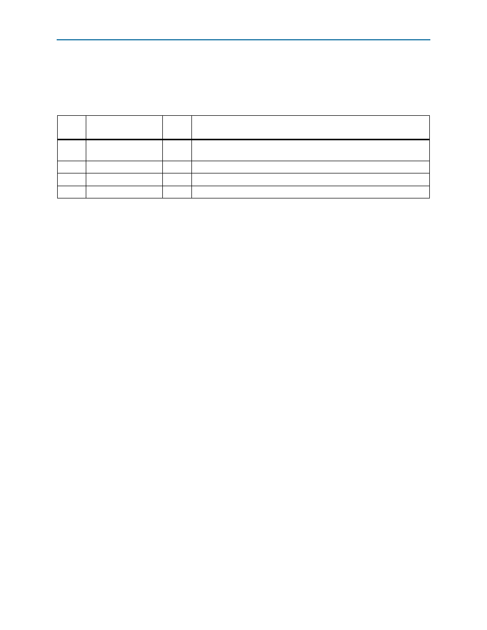
Table 17–18. DMA Control Register Setup for DMA Read
Offset in DMA Control
Registers (BAR2)
Value
Description
DW0
0x0
3
Number of descriptors and control bits as described in
DW1
0x14
0
BFM shared memory upper address value
DW2
0x18
0x900
BFM shared memory lower address value
DW3
0x1c
2
Last descriptor written