Avalon-mm interface, Off-chip sdram interface, Signal timing and electrical characteristics – Altera Embedded Peripherals IP User Manual
Page 18: Avalon-mm interface -2, Off-chip sdram interface -2
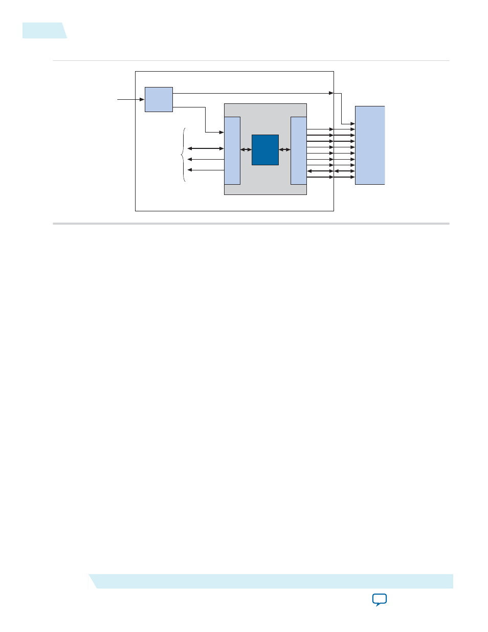
Figure 2-1: SDRAM Controller with Avalon Interface Block Diagram
Avalon-MM slave
interface
to on-chip
logic
SDRAM Controller Core
data, control
A
valon-MM Sla
ve P
or
t
clock
waitrequest
readdatavalid
dq
dqm
PLL
Phase Shift
Interf
ace to SDRAM pins
Altera FPGA
clk
addr
ras
cas
cs
cke
ba
we
Control
Logic
address
SDRAM Clock
Controller Clock
Clock
Source
SDRAM Chip
(PC100)
The following sections describe the components of the SDRAM controller core in detail. All options are
specified at system generation time, and cannot be changed at runtime.
Avalon-MM Interface
The Avalon-MM slave port is the user-visible part of the SDRAM controller core. The slave port presents
a flat, contiguous memory space as large as the SDRAM chip(s). When accessing the slave port, the details
of the PC100 SDRAM protocol are entirely transparent. The Avalon-MM interface behaves as a simple
memory interface. There are no memory-mapped configuration registers.
The Avalon-MM slave port supports peripheral-controlled wait states for read and write transfers. The
slave port stalls the transfer until it can present valid data. The slave port also supports read transfers with
variable latency, enabling high-bandwidth, pipelined read transfers. When a master peripheral reads
sequential addresses from the slave port, the first data returns after an initial period of latency. Subsequent
reads can produce new data every clock cycle. However, data is not guaranteed to return every clock cycle,
because the SDRAM controller must pause periodically to refresh the SDRAM.
For details about Avalon-MM transfer types, refer to the
Off-Chip SDRAM Interface
The interface to the external SDRAM chip presents the signals defined by the PC100 standard. These
signals must be connected externally to the SDRAM chip(s) through I/O pins on the Altera device.
Signal Timing and Electrical Characteristics
The timing and sequencing of signals depends on the configuration of the core. The hardware designer
configures the core to match the SDRAM chip chosen for the system. See the Configuration section for
details. The electrical characteristics of the device pins depend on both the target device family and the
assignments made in the Quartus
®
II software. Some device families support a wider range of electrical
2-2
Avalon-MM Interface
UG-01085
2014.24.07
Altera Corporation
SDRAM Controller Core