Block diagram, Configuration parameter, Block diagram -2 – Altera Embedded Peripherals IP User Manual
Page 32: Configuration parameter -2, Timing page
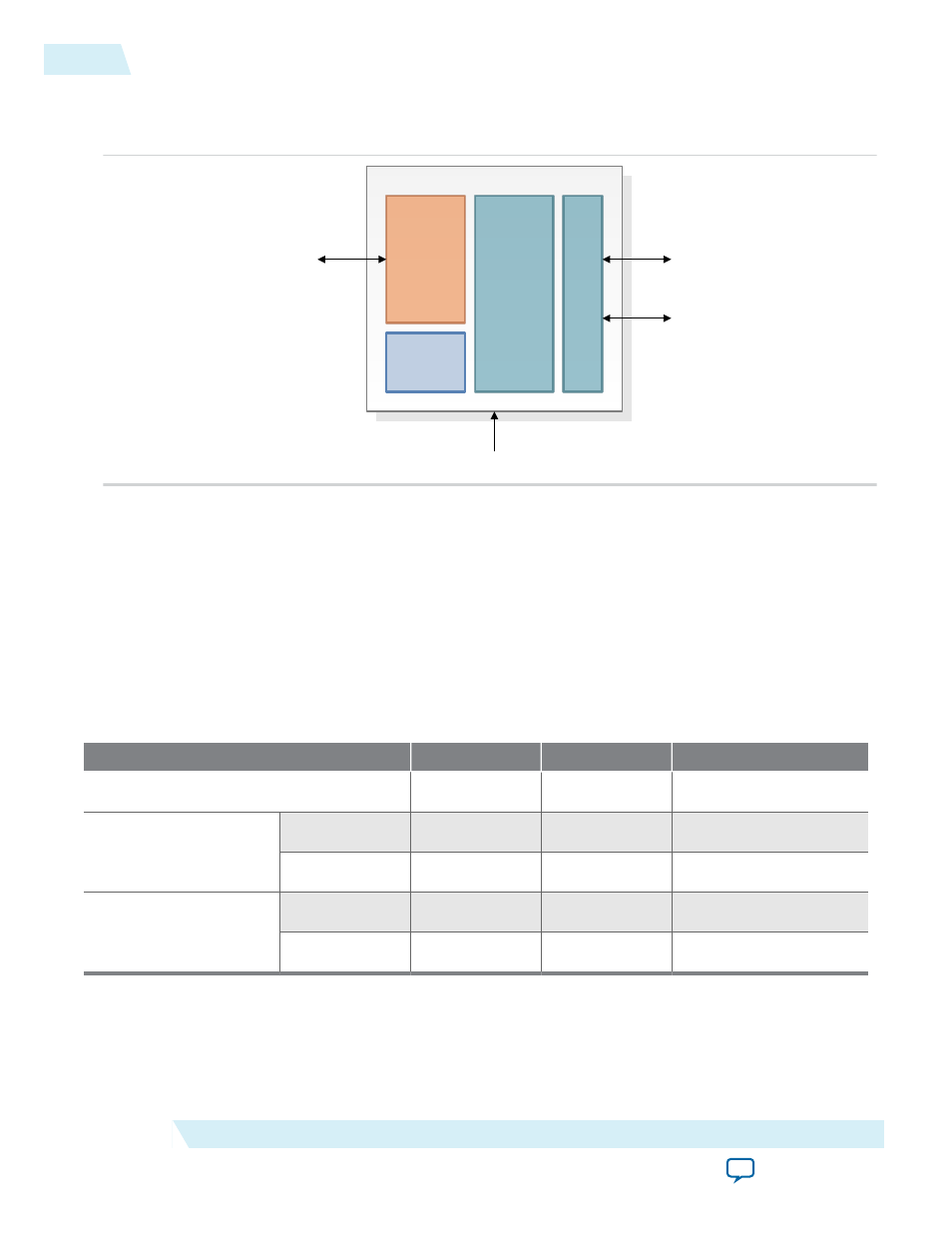
Block Diagram
Figure 3-1: Tri-State SDRAM Block Diagram
altera _sdram _controller
Init FSM
Request
Buffer
Avalon-MM
Interface
SDRAM
Interface
Main
FSM
Signal Generation
Clock / Reset
Tri-state
Conduit
Master Signals
Configuration Parameter
The following table shows the configuration parameters available for user to program during generation
time of the IP core.
Memory Profile Page
The Memory Profile page allows you to specify the structure of the SDRAM subsystem such as address
and data bus widths, the number of chip select signals, and the number of banks.
Table 3-1: Configuration Parameters
Parameter
GUI Legal Values
Default Values
Units
Data Width
8, 16, 32, 64
32
(Bit)s
Architecture
Chip Selects
1, 2, 4, 8
1
(Bit)s
Banks
2, 4
4
(Bit)s
Address Widths
Row
11:14
12
(Bit)s
Column
8:14
8
(Bit)s
Timing Page
The Timing page allows designers to enter the timing specifications of the Tri-State SDRAM chip(s) used.
The correct values are available in the manufacturer’s data sheet for the target SDRAM.
3-2
Block Diagram
UG-01085
2014.24.07
Altera Corporation
Tri-State SDRAM