Implementation details, Interrupt latency counter architecture, Implementation details -7 – Altera Embedded Peripherals IP User Manual
Page 335: Interrupt latency counter architecture -7
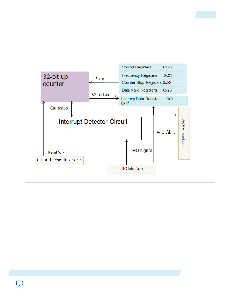
Implementation Details
Interrupt Latency Counter Architecture
Figure 34-2: Interrupt Latency Calculator Architecture
The interrupt latency calculator operates on a single clock domain which is determined by which clock it
is receiving at the CLK interface. The interrupt detector circuit is made up of a positive-edge triggered
flop which delays the IRQ signal to be XORed with the original signal. The pulse resulted from the
previous operation is then fed to an enable register where it will switch its state from logic ‘low’ to ‘high’.
This will trigger the counter to start its operation. Prior to this, the reset signal is assumed to be triggered
through the firmware. Once the Interrupt service routine has been completed, the IRQ signal drops to
logic low. This causes another pulse to be generated to stop the counter. Data from the counter is then
duplicated into the latency data register to be read out.
When the interrupt detector is configured to react to a pulse signal, the incoming pulse is fed directly to
enable the register to turn on the counter. In this mode, to halt the counter’s operation, you have to write
a Boolean ‘1’ to the counter stop bit. Only the first IRQ pulse can trigger the counter to start counting and
that subsequent pulse will not cause the counter to reset until a Boolean ‘1’ is written into the counter stop
register. In ‘pulse’ mode, the latency measured by the IP is one clock cycle more than actual latency.
UG-01085
2014.24.07
Implementation Details
34-7
Altera Interrupt Latency Counter
Altera Corporation