Altera Embedded Peripherals IP User Manual
Page 21
controller core easily by selecting the appropriate preset value. The following preset configurations are
defined:
• Micron MT8LSDT1664HG module
• Four SDR100 8 MByte × 16 chips
• Single Micron MT48LC2M32B2-7 chip
• Single Micron MT48LC4M32B2-7 chip
• Single NEC D4564163-A80 chip (64 MByte × 16)
• Single Alliance AS4LC1M16S1-10 chip
• Single Alliance AS4LC2M8S0-10 chip
Selecting a preset configuration automatically changes values on the Memory Profile and Timing tabs
to match the specific configuration. Altering a configuration setting on any page changes the Preset
value to custom.
Memory Profile Page
The Memory Profile page allows you to specify the structure of the SDRAM subsystem such as address
and data bus widths, the number of chip select signals, and the number of banks.
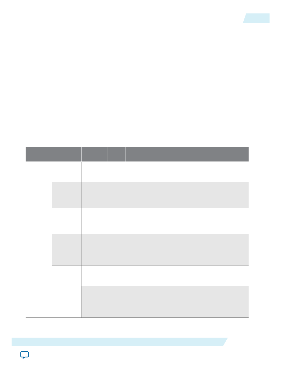
Table 2-1: Memory Profile Page Settings
Settings
Allowed
Values
Default
Values
Description
Data Width
8, 16, 32,
64
32
SDRAM data bus width. This value determines the
width of the
dq
bus (data) and the
dqm
bus (byte-
enable).
Archite
cture
Setting
s
Chip Selects 1, 2, 4, 8
1
Number of independent chip selects in the SDRAM
subsystem. By using multiple chip selects, the
SDRAM controller can combine multiple SDRAM
chips into one memory subsystem.
Banks
2, 4
4
Number of SDRAM banks. This value determines the
width of the
ba
bus (bank address) that connects to
the SDRAM. The correct value is provided in the data
sheet for the target SDRAM.
Addres
s
Width
Setting
s
Row
11, 12, 13,
14
12
Number of row address bits. This value determines
the width of the
addr
bus. The Row and Column
values depend on the geometry of the chosen
SDRAM. For example, an SDRAM organized as 4096
(2
12
) rows by 512 columns has a Row value of 12.
Column
>= 8, and
less than
Row value
8
Number of column address bits. For example, the
SDRAM organized as 4096 rows by 512 (2
9
) columns
has a Column value of 9.
Share pins via tri-
state bridge dq/dqm/
addr I/O pins
On, Off
Off
When set to No, all pins are dedicated to the SDRAM
chip. When set to Yes, the
addr
,
dq
, and
dqm
pins can
be shared with a tristate bridge in the system. In this
case, select the appropriate tristate bridge from the
pull-down menu.
UG-01085
2014.24.07
Memory Profile Page
2-5
SDRAM Controller Core
Altera Corporation