Software programming model, Clock, pll and timing considerations, Factors affecting sdram timing – Altera Embedded Peripherals IP User Manual
Page 25: Software programming model -9, Clock, pll and timing considerations -9, Factors affecting sdram timing -9
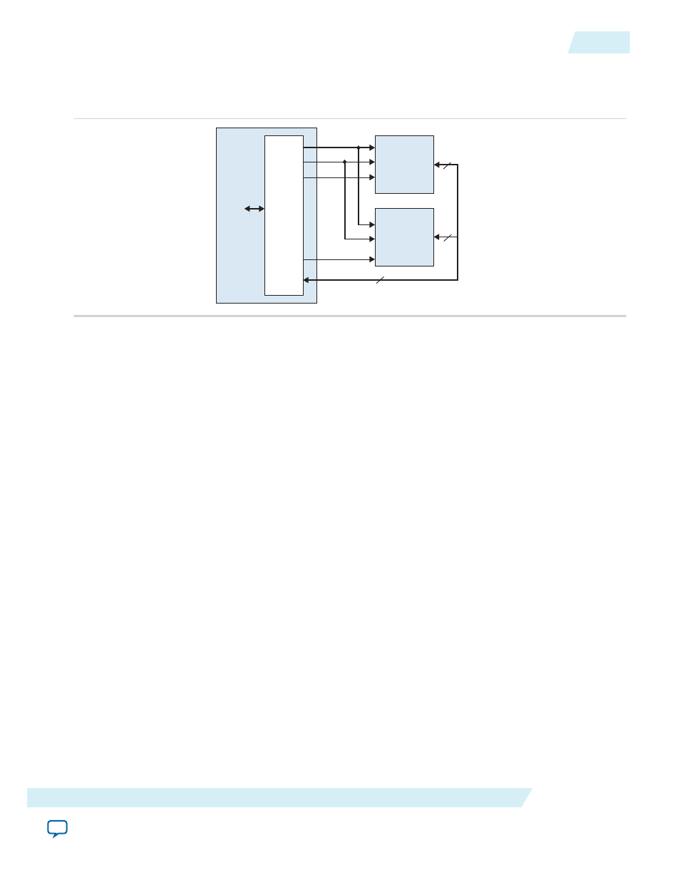
The address, data, and control signals connect in parallel to the two chips. The chipselect bus (
cs_n[1:0]
)
determines which chip is selected. The result is a logical 256-Mbit 32-bit wide memory.
Figure 2-4: Two 128-Mbit SDRAM Chips Each with 32-Bit Data
addr
ctl
cs_n [0]
cs_n [1]
SDRAM
Controller
Altera FPGA
Avalon-MM
interface
to
on-chip
logic
data
32
128 Mbits
16 Mbytes
32 data width device
128 Mbits
16 Mbytes
32 data width device
32
32
Software Programming Model
The SDRAM controller behaves like simple memory when accessed via the Avalon-MM interface. There
are no software-configurable settings and no memory-mapped registers. No software driver routines are
required for a processor to access the SDRAM controller.
Clock, PLL and Timing Considerations
This section describes issues related to synchronizing signals from the SDRAM controller core with the
clock that drives the SDRAM chip. During SDRAM transactions, the address, data, and control signals are
valid at the SDRAM pins for a window of time, during which the SDRAM clock must toggle to capture
the correct values. At slower clock frequencies, the clock naturally falls within the valid window. At higher
frequencies, you must compensate the SDRAM clock to align with the valid window.
Determine when the valid window occurs either by calculation or by analyzing the SDRAM pins with an
oscilloscope. Then use a PLL to adjust the phase of the SDRAM clock so that edges occur in the middle of
the valid window. Tuning the PLL might require trial-and-error effort to align the phase shift to the
properties of your target board.
For details about the PLL circuitry in your target device, refer to the appropriate device family handbook.
For details about configuring the PLLs in Altera devices, refer to the
Factors Affecting SDRAM Timing
The location and duration of the window depends on several factors:
UG-01085
2014.24.07
Software Programming Model
2-9
SDRAM Controller Core
Altera Corporation