Timing and fmax, Timing and fmax -6 – Altera Embedded Peripherals IP User Manual
Page 92
Resource
Number
Routing optimization registers
17
Global Signals
2
M10k blocks
0
Total MLAB memory bits
2432
Timing and Fmax
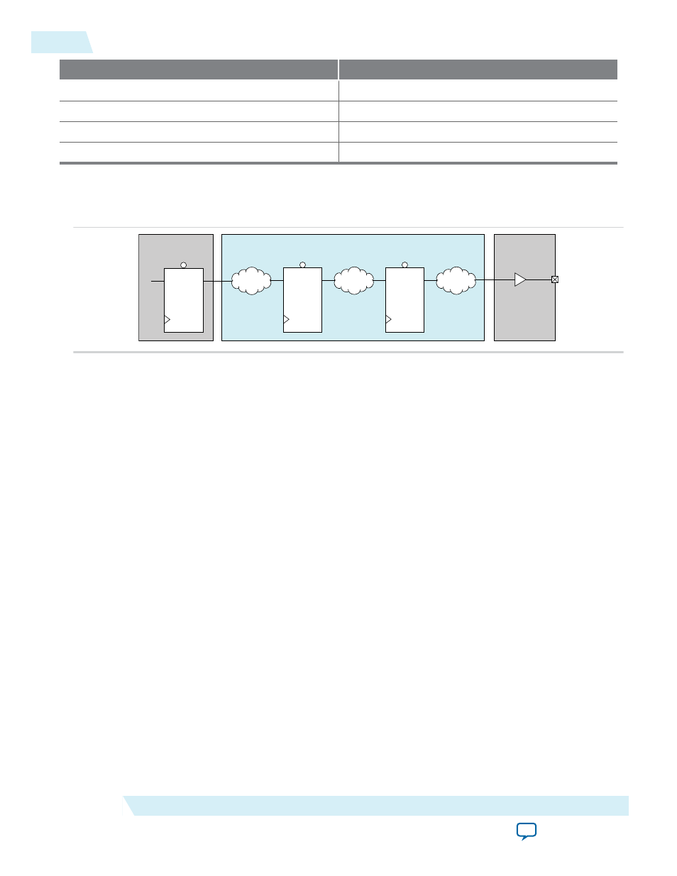
Figure 9-2: Maximum Delays on UART
External Pin
UART IP Core
D
Q
Avalon Master
D
Q
D
Q
4 ns
2 ns
8 ns
7 ns
COMBI
COMBI
COMBI
The diagram above shows worst case combinatorial delays throughout the UART IP Core. These
estimates are provided by TimeQuest under the following condition:
• Device Family: Series V and above
• Avalon Master connected to Avalon Slave port of the UART with outputs from the Avalon Master
registered
• RS-232 Serial Interface is exported to FPGA Pin
• Clocks for entire system set at 125 MHz
Based on the conditions above the UART IP has an Fmax value of 125 MHz, with the worst delay being
internal register-to-register paths.
The UART has combinatorial logic on both the Input and Output side, with system level implications on
the Input side.
The Input side combinatorial logic (with 7ns delay) goes through the Avalon address decode logic, to the
Read data output registers. It is therefore recommended that Masters connected to the UART IP register
their output signals.
The Output side combinatorial logic (with 2ns delay) goes through the RS-232 Serial Output. There
shouldn’t be any concern on the output side delays though – as it is not a single cycle path. Using the
highest clock divider value of 1, the serial output only toggles once every 16 clocks. This naturally gives a
9-6
Timing and Fmax
UG-01085
2014.24.07
Altera Corporation
16550 UART