Altera Embedded Peripherals IP User Manual
Page 254
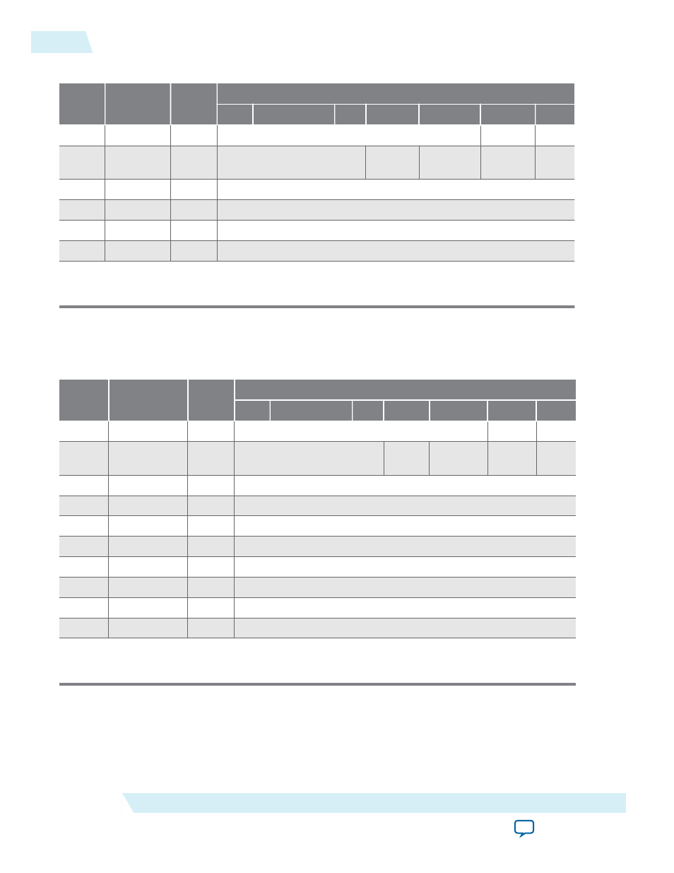
Table 25-3: Register Map—32-bit Timer
Offset
Name
R/W
Description of Bits
15
...
4
3
2
1
0
0
status
RW
RUN
TO
1
control
RW
STOP
START
CONT
IT
O
2
periodl
RW
Timeout Period – 1 (bits [15:0])
3
periodh
RW
Timeout Period – 1 (bits [31:16])
4
snapl
RW
Counter Snapshot (bits [15:0])
5
snaph
RW
Counter Snapshot (bits [31:16])
1. Reserved. Read values are undefined. Write zero.
.
Table 25-4: Register Map—64-bit Timer
Offset
Name
R/W
Description of Bits
15
...
4
3
2
1
0
0
status
RW
RUN
TO
1
control
RW
STOP
START
CONT
IT
O
2
period_0
RW
Timeout Period – 1 (bits [15:0])
3
period_1
RW
Timeout Period – 1 (bits [31:16])
4
period_2
RW
Timeout Period – 1 (bits [47:32])
5
period_3
RW
Timeout Period – 1 (bits [63:48])
6
snap_0
RW
Counter Snapshot (bits [15:0])
7
snap_1
RW
Counter Snapshot (bits [31:16])
8
snap_2
RW
Counter Snapshot (bits [47:32])
9
snap_3
RW
Counter Snapshot (bits [63:48])
1. Reserved. Read values are undefined. Write zero.
status Register
The
status
register has two defined bits.
25-6
Register Map
UG-01085
2014.24.07
Altera Corporation
Interval Timer Core