Example calculation, Example calculation -11 – Altera Embedded Peripherals IP User Manual
Page 27
Advertising
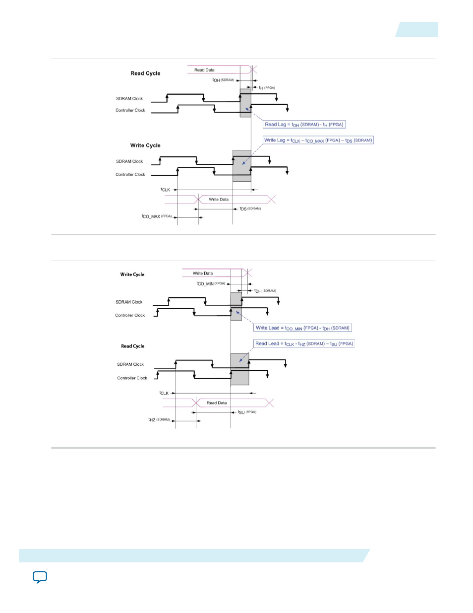
Figure 2-5: Calculating the Maximum SDRAM Clock Lag
Figure 2-6: Calculating the Maximum SDRAM Clock Lead
Example Calculation
This section demonstrates a calculation of the signal window for a Micron MT48LC4M32B2-7 SDRAM
chip and design targeting the Stratix II EP2S60F672C5 device. This example uses a CAS latency (CL) of 3
cycles, and a clock frequency of 50 MHz. All SDRAM signals on the device are registered in I/O cells,
enabled with the Fast Input Register and Fast Output Register logic options in the Quartus II software.
UG-01085
2014.24.07
Example Calculation
2-11
SDRAM Controller Core
Altera Corporation
Advertising