Z80x30 write cycle timing – Zilog Z80230 User Manual
Page 25
Advertising
SCC/ESCC
User Manual
UM010903-0515
Interfacing the SCC/ESCC
18
Z80X30 Read Cycle
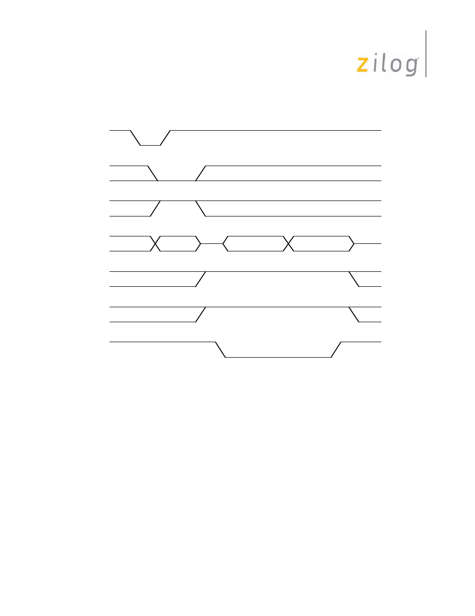
Z80X30 Write Cycle Timing
The write cycle timing for the Z80X30 is displayed in
on page 19. The register address on
AD7-AD0, as well as the state of /CS0 and /INTACK, are latched by the rising edge of /AS. R//W
must be Low when /DS falls to indicate a write cycle. The leading edge of the coincidence of CS1
High and /DS Low latches the write data on AD7-AD0, as well as the state of R//W.
/AS
/CS0
/INTACK
AD7 - AD0
R//W
CS1
/DS
Address
Data Valid
Advertising