Z85x30 read cycle timing, Z85x30 write cycle timing – Zilog Z80230 User Manual
Page 35
SCC/ESCC
User Manual
UM010903-0515
Interfacing the SCC/ESCC
28
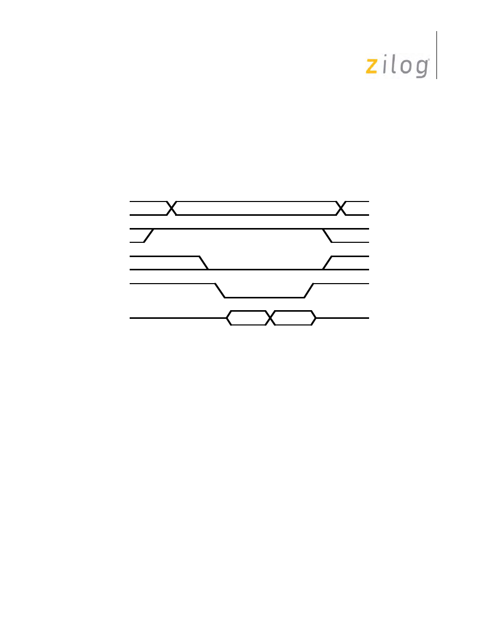
Z85X30 Read Cycle Timing
The read cycle timing for the Z85X30 is displayed in
on page 28. The address on A//B and
D//C is latched by the coincidence of /RD and /CE active. /CE must remain Low and /INTACK
must remain High throughout the cycle. The Z85X30 bus drivers are enabled while /CE and /RD
are both Low. A read with D//C High does not disturb the state of the pointers and a read cycle
with D//C Low resets the pointers to zero after the internal operation is complete
Z85X30 Read Cycle Timing
Z85X30 Write Cycle Timing
The write cycle timing for the Z85X30 is displayed in
on page 29. The address on A//B
and D//C, as well as the data on D7-D0, is latched by the coincidence of /WR and /CE active. /CE
must remain Low and /INTACK must remain High throughout the cycle. A write cycle with D//C
High does not disturb the state of the pointers and a write cycle with D//C Low resets the pointers
to zero after the internal operation is complete.
Historically, the NMOS/CMOS version latched the data bus on the falling edge of /WR. However,
many CPUs do not guarantee that the data bus is valid at the time when the /WR pin goes low, so
the data bus timing was modified to allow a maximum delay from the falling edge of /WR to the
latching of the data bus. On the Z85230/L, the AC Timing parameter #29 TsDW(WR), Write Data
to /WR falling minimum, has been changed to: /WR falling to Write Data Valid maximum. Refer
to the AC Timing Characteristic section of the Z85230/L Product Specification for more informa-
tion regarding this change.
A//B, D//C
/INTACK
/CE
/RD
D7-D0
Address Valid
Data Valid