Figure, Scc/escc user manual – Zilog Z80230 User Manual
Page 93
Advertising
SCC/ESCC
User Manual
UM010903-0515
SCC/ESCC Ancillary Support Circuitry
86
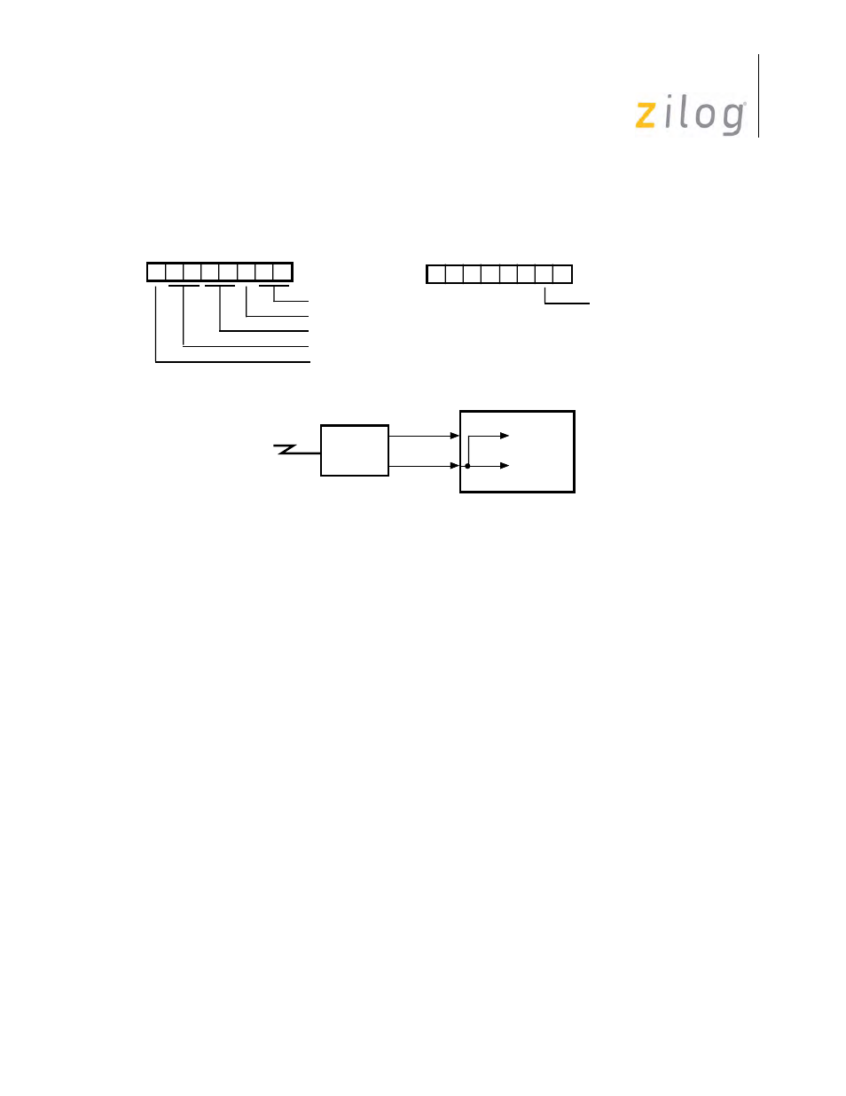
Clock Source Selection
on page 87 displays the use of the DPLL to derive a 1x clock from the data. In this exam-
ple:
The DPLL clock input = BRG output (x16 the data rate) WR14.
The DPLL clock output = RxC (receiver clock) WR11.
Set FM mode WR14.
Set FM mode WR10.
0
WR14
BRG Clock Source = /RTXC
or XTAL OSCILLATOR
D1
D7
D0
WR11
/TRxC OUT = BRG Output
/TRxC Pin = Output Pin
Tx Clock = BRG Output
Rx Clock = BRG Output
Using External Crystal
1
1
0
1
0
1
1
0
SCC
NRZ Data
RxD Pin
SYNC
Modem
/RTxC Pin
RxC
TxC
1x
Advertising