Altera IP Compiler for PCI Express User Manual
Page 175
Chapter 7: Reset and Clocks
7–11
Clocks
August 2014
Altera Corporation
IP Compiler for PCI Express User Guide
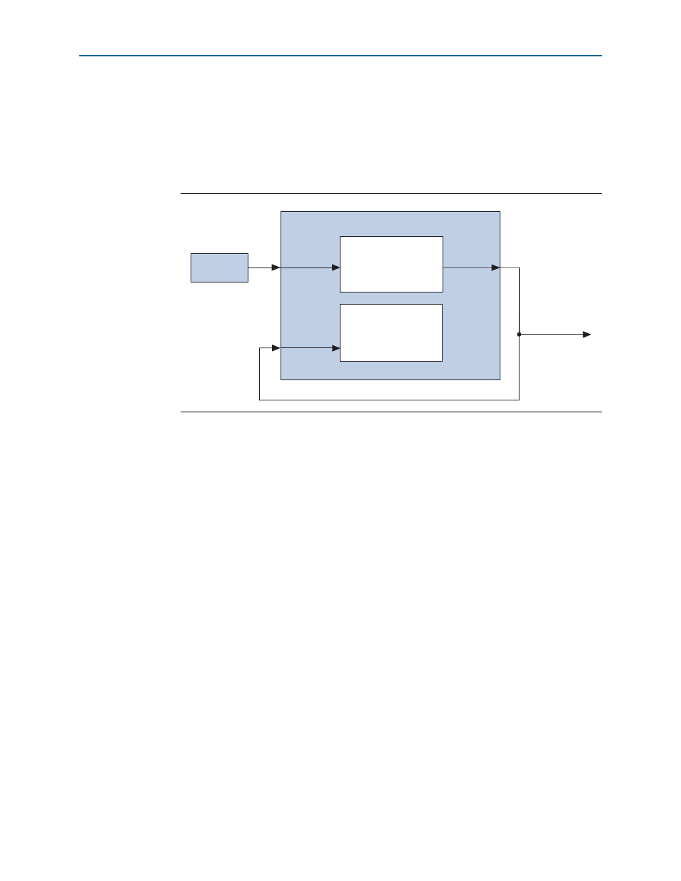
Clocking for a Generic PIPE PHY and the Simulation Testbench
illustrates the clocking when the PIPE interface is used. The same
configuration is also used for simulation. As this figure illustrates the 100 MHz
reference clock drives the input to a PLL which creates a 125 MHz clock for both the
IP Compiler for PCI Express and the application logic.
Avalon-MM Interface–Hard IP and Soft IP Implementations
When using the IP Compiler for PCI Express with an Avalon-MM application
interface in the Qsys design flow, the clocking is the same for both the soft IP and hard
IP implementations. The clocking requirements explained in the previous sections
remain valid. The IP Compiler for PCI Express with Avalon-MM interface supports
two clocking modes:
■
Separate PCI Express and Avalon clock domains
■
Single PCI Express core clock as the system clock for the Avalon-MM clock domain
The IP Compiler for PCI Express exports a 125 MHz clock, clk125_out, which can be
used for logic outside the IP core. This clock is not visible to Qsys and therefore cannot
drive other Avalon-MM components in the system.
The Qsys design flow does not allow you to select the clocking mode. A
Qsys-generated IP Compiler for PCI Express implements the single clock domain
mode.
I
Figure 7–8. Clocking for the Generic PIPE Interface and the Simulation Testbench, All Device
Families
100-MHz
Clock Source
refclk
clk125_out
Application Clock
core_clk_out
PLL
<variant>.v or .vhd - For Simulation
<variant>
_core.v or .vhd
(IP Compiler for PCI Express)
pll_inclk
pld_clk