Transaction examples using receive signals, Transaction without data payload, Transaction aborted – Altera IP Compiler for PCI Express User Manual
Page 324: Transaction with data payload, Transaction with data payload and wait states, Dependencies between receive signals
B–6
Chapter :
Descriptor/Data Interface
IP Compiler for PCI Express User Guide
August 2014
Altera Corporation
Transaction Examples Using Receive Signals
This section provides the following additional examples that illustrate how
transaction signals interact:
■
Transaction without Data Payload
■
Retried Transaction and Masked Non-Posted Transactions
■
■
■
Transaction with Data Payload and Wait States
■
Dependencies Between Receive Signals
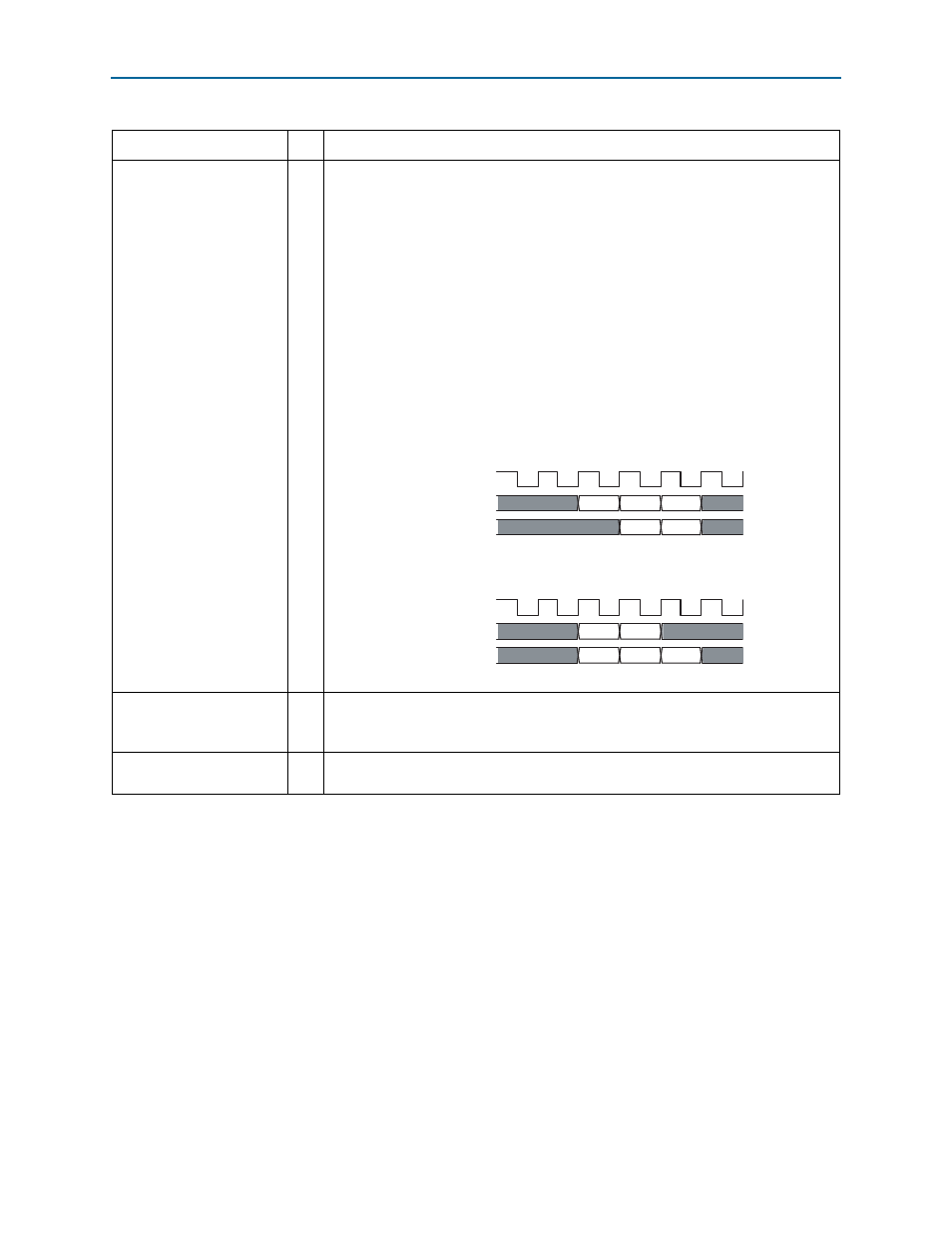
rx_data<n>[63:0]
O
Receive data bus. This bus transfers data from the link to the application layer. It is 2
DWORDS wide and is naturally aligned with the address in one of two ways, depending
on bit 2 of rx_desc.
■
rx_desc[2] (64-bit address) when 0: The first DWORD is located on rx_data[31:0].
■
rx_desc[34] (32-bit address) when 0: The first DWORD is located on bits
rx_data[31:0].
■
rx_desc[2] (64-bit address) when 1: The first DWORD is located on bits
rx_data[63:32].
■
rx_desc[34] (32-bit address) when 1: The first DWORD is located on bits
rx_data[63:32].
This natural alignment allows you to connect rx_data[63:0] directly to a 64-bit datapath
aligned on a QW address (in the little endian convention).
Bit 2 is set to 1 (5 DWORD transaction)
Figure B–3.
Bit 2 is set to 0 (5 DWORD transaction)
Figure B–4.
rx_be<n>[7:0]
O
Receive byte enable. These signals qualify data on rx_data[63:0]. Each bit of the
signal indicates whether the corresponding byte of data on rx_data[63:0] is valid.
These signals are not available in the ×8 IP core.
rx_ws<n>
I
Receive wait states. With this signal, the application layer can insert wait states to
throttle data transfer.
Note to
(1) For all signals, <n> is the virtual channel number which can be 0 or 1.
Table B–4. RX Data Phase Signals (Part 2 of 2)
Signal
I/O
Description
clk
rx_data[63:32]
rx_data[31:0]
DW 0
DW 2
DW 4
DW 1
DW 3
1
2
3
4
5
6
clk
rx_data[63:32]
rx_data[31:0]
DW 1
DW 3
DW 0
DW 2
DW 4
1
2
3
4
5
6