Transaction with data payload and wait states – Altera IP Compiler for PCI Express User Manual
Page 328
B–10
Chapter :
Descriptor/Data Interface
IP Compiler for PCI Express User Guide
August 2014
Altera Corporation
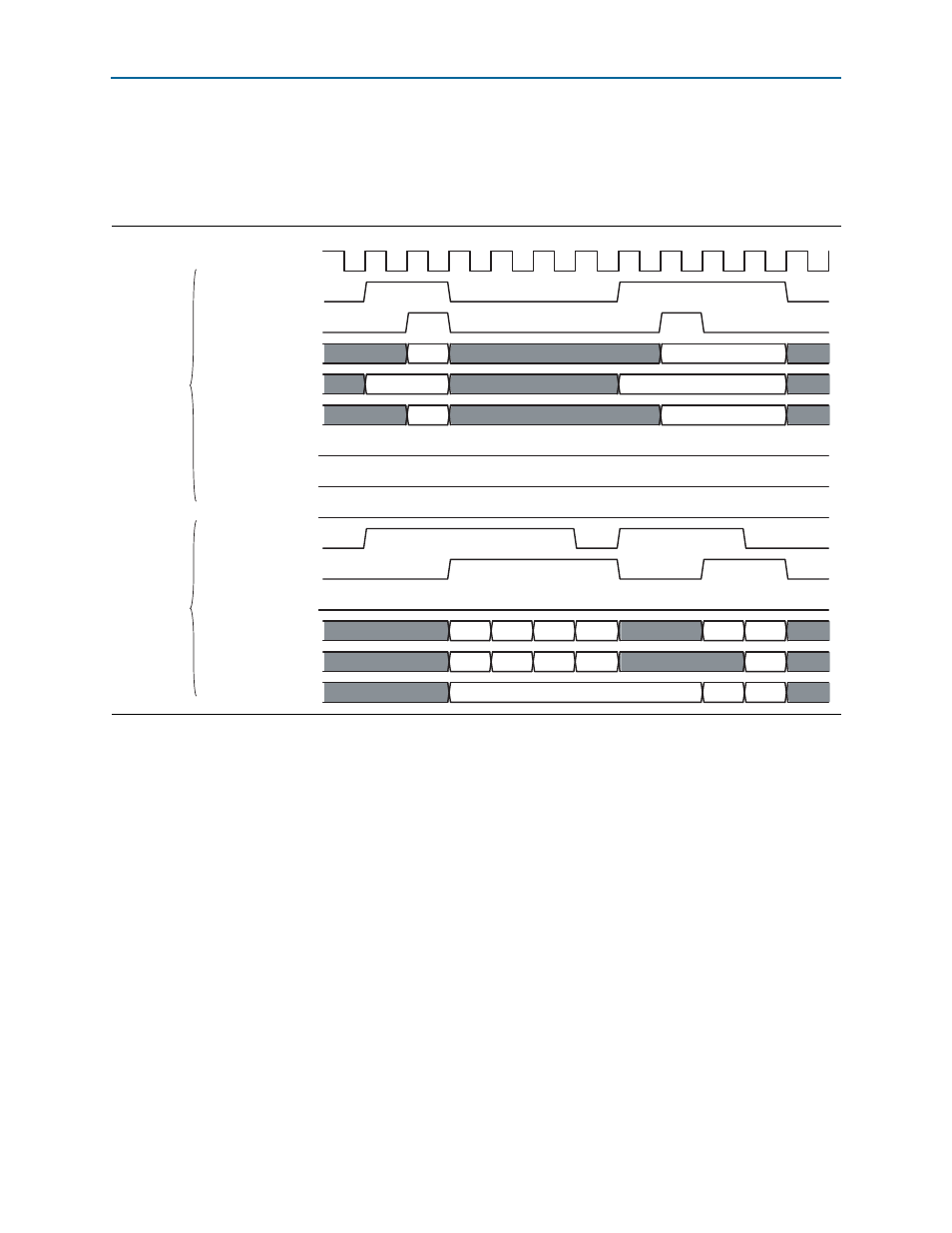
Normally, rx_dfr is asserted on the same or following clock cycle as rx_req; however,
in this case the signal is already asserted until clock cycle 7 to signal the end of
transmission of the first transaction. It is immediately reasserted on clock cycle eight
to request a data phase for the second transaction.
Transaction with Data Payload and Wait States
The application layer can assert rx_ws without restrictions. In
, the IP core
receives a completion transaction of four DWORDS. Bit 2 of rx_data[63:0] is set to 1.
Both the application layer and the IP core insert wait states. Normally rx_data[63:0]
would contain data in clock cycle 4, but the IP core has inserted a wait state by
deasserting rx_dv.
In clock cycle 11, data transmission does not resume until both of the following
conditions are met:
■
The IP core asserts rx_dv at clock cycle 10, thereby ending a IP core-induced wait
state.
Figure B–8. RX Transaction with a Data Payload Waveform
clk
rx_req
rx_ack
rx_desc[135:128]
rx_desc[127:64]
rx_desc[63:0]
rx_abort
rx_retry
rx_mask
rx_dfr
rx_dv
rx_ws
rx_data[63:32]
rx_data[31:0]
rx_be[7:0]
valid
valid
CPLD 8 DW
MEMWR/AD 3 DW
valid
valid
DW 1
DW 3
DW 5
DW 7
DW 0
DW 2
DW 0
DW 2
DW 4
DW 6
DW 1
0xFF
0x0F
0xFF
1
2
3
4
5
6
7
8
9
10
11
12
Descriptor
Signals
Data
Signals