Altera IP Compiler for PCI Express User Manual
Page 338
B–20
Chapter :
Descriptor/Data Interface
IP Compiler for PCI Express User Guide
August 2014
Altera Corporation
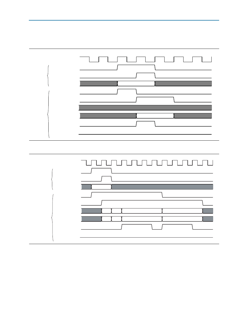
shows how the transaction layer extends the a data phase by asserting the
wait state signal.
Transaction Layer Inserts Wait States because of Four Dword Header
In this example, the application transmits a 64-bit memory write transaction. Address
bit 2 is set to 1. Refer to
. No wait states are inserted during the first two
data phases because the IP core implements a small buffer to give maximum
performance during transmission of back-to-back transaction layer packets.
Figure B–16. TX Transfer with Wait State Inserted for a Single DWORD Write
Figure B–17. TX Signal Activity When IP core Has Fewer than Maximum Potential Lanes Waveform
clk
tx_req
tx_ack
tx_desc[127:0]
tx_dfr
tx_dv
tx_data[63:32]
tx_data[31:0]
tx_ws
tx_err
MEMWR32
DW0
1
2
3
4
5
6
7
Descriptor
Signals
Data
Signals
clk
tx_req
tx_ack
tx_desc[127:0]
tx_dfr
tx_dv
tx_data[63:32]
tx_data[31:0]
tx_ws
tx_err
MEMWR32
DW 1
DW 3
DW 5
DW 7
DW 0
DW 2
DW 4
DW 6
1
2
3
4
5
6
7
8
9
10
11
12
13
Descriptor
Signals
Data
Signals