Altera IP Compiler for PCI Express User Manual
Page 353
Chapter :
B–35
Recommended Incremental Compilation Flow
August 2014
Altera Corporation
IP Compiler for PCI Express User Guide
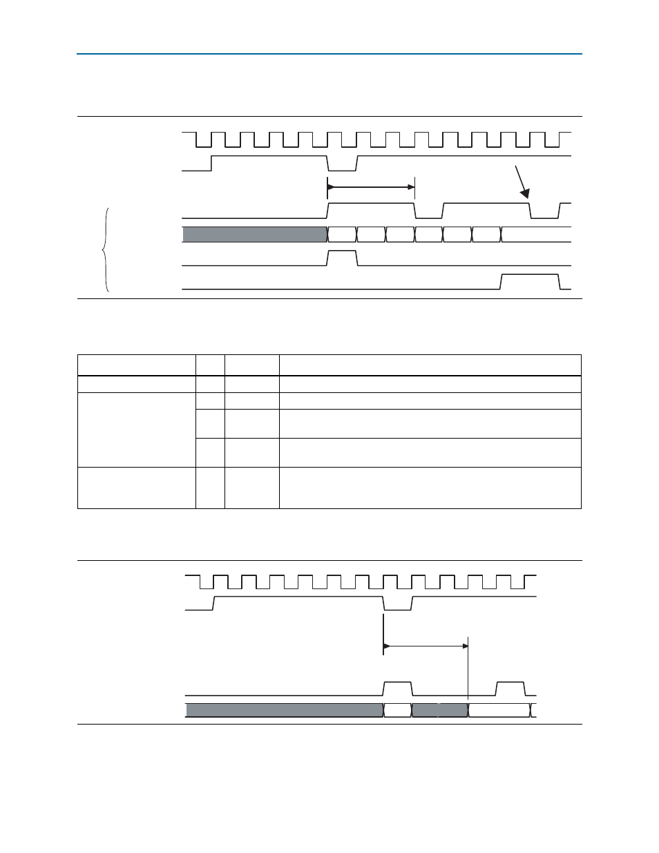
shows the application-side TX interface timing diagram.
describes the MSI TX signals.
shows the application-side MSI interface timing diagram.
Figure B–26. TX Interface Timing Diagram
clk
tx_stream_ready0
tx_stream_valid0
tx_desc0
tx_sop_flag
tx_eop_flag
desc_hi desc_lo
data0
data1
last data
tx_data0
tx_s
tr
e
a
m_data0
1
2
3
4
5
6
7
8
9
10
11
12
13
14
allowed
response time
0 - 3 clocks
source
throttles
data
Table B–16. MSI TX Signals
Signal
Bit
Subsignals
Description
msi_stream_valid0
Clocks
msi_st_data
into the ICM.
msi_stream_data0
63:8
msi data.
7:5
Corresponds to the app_msi_tc signal on the IP core. Refer to
for more information.
4:0
Corresponds to the app_msi_num signal on the IP core. Refer to
for more information.
msi_stream_ready0
The ICM asserts this signal when it can accept more MSI requests. When
deasserted, the application must deassert msi_st_valid within 3 CLK
cycles.
Figure B–27. MSI Interface Timing Diagram
clk
msi_stream_ready0
msi_stream_valid0
msi_stream_data0
msi1
msi2
1
2
3
4
5
6
7
8
9
10
11
12
13
allowed
response time
0 - 3 clocks