Throughput of non-posted reads, Note 1), Note 2) – Altera IP Compiler for PCI Express User Manual
Page 200
11–4
Chapter 11: Flow Control
Throughput of Non-Posted Reads
IP Compiler for PCI Express User Guide
August 2014
Altera Corporation
Based on the above FC Update Loop delays and additional arbitration and packet
length delays,
shows the number of flow control credits that must be
advertised to cover the delay. The RX buffer size must support this number of credits
to maintain full bandwidth.
These numbers take into account the device delays at both ends of the PCI Express
link. Different devices at the other end of the link could have smaller or larger delays,
which affects the minimum number of credits required. In addition, if the application
layer cannot drain received packets immediately in all cases, it may be necessary to
offer additional credits to cover this delay.
Setting the Desired performance for received requests to High on the Buffer Setup
page on the Parameter Settings tab using the parameter editor configures the RX
buffer with enough space to meet the above required credits. You can adjust the
Desired performance
for received request up or down from the High setting to tailor
the RX buffer size to your delays and required performance.
Throughput of Non-Posted Reads
To support a high throughput for read data, you must analyze the overall delay from
the time the application layer issues the read request until all of the completion data is
returned. The application must be able to issue enough read requests, and the read
completer must be capable of processing these read requests quickly enough (or at
least offering enough non-posted header credits) to cover this delay.
However, much of the delay encountered in this loop is well outside the IP Compiler
for PCI Express and is very difficult to estimate. PCI Express switches can be inserted
in this loop, which makes determining a bound on the delay more difficult.
From receipt of FC Update DLLP on the PCI
Express Link to updating of transmitter's Credit
Limit register.
116
160
184
232
424
472
Notes to
:
(1) The numbers for other Gen1 PHYs are similar.
(2) Gen2 numbers are to be determined.
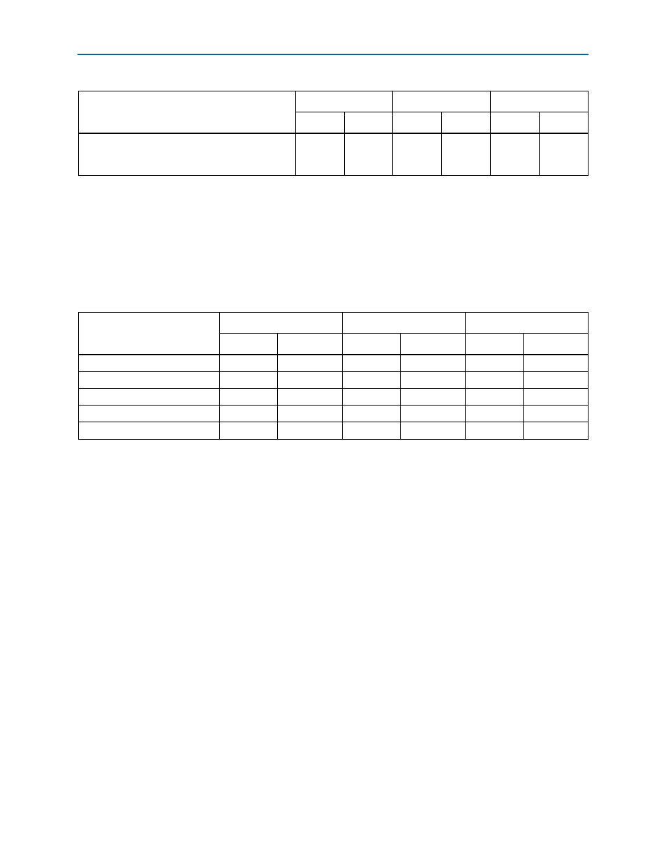
Table 11–1. FC Update Loop Delay in Nanoseconds Components For Stratix II GX (Part 2 of 2)
(Note 1)
,
(Note 2)
Delay Path
×8 Function
×4 Function
×1 Function
Min
Max
Min
Max
Min
Max
Table 11–2. Data Credits Required By Packet Size
Max Packet Size
×8 Function
×4 Function
×1 Function
Min
Max
Min
Max
Min
Max
128
64
96
56
80
40
48
256
80
112
80
96
64
64
512
128
160
128
128
96
96
1024
192
256
192
192
192
192
2048
384
384
384
384
384
384