Altera IP Compiler for PCI Express User Manual
Page 350
B–32
Chapter :
Incremental Compile Module for Descriptor/Data Examples
IP Compiler for PCI Express User Guide
August 2014
Altera Corporation
RX Ports
describes the application-side ICM RX signals.
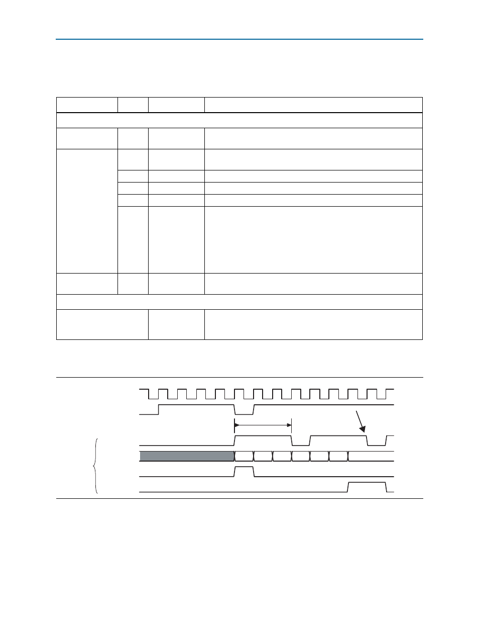
shows the application-side RX interface timing diagram.
Table B–14. Application-Side RX Signals
Signal Bits
Subsignals
Description
Interface Signals
rx_st_valid0
Clocks rx_st_data into the application. The application must accept the
data when rx_st_valid is high.
rx_st_data0
[81:74]
Byte Enable bits
Byte-enable bits. These are valid on the data (3rd to last) cycles of the
packet.
[73]
rx_sop_flag
When asserted, indicates that this is the first cycle of the packet.
[72]
rx_eop_flag
When asserted, indicates that this is the last cycle of the packet.
[71:64]
Bar bits
BAR bits. These are valid on the 2nd cycle of the packet.
[63:0]
rx_desc/rx_data
Multiplexed rx_desc/rx_data bus
1st cycle – rx_desc0[127:64]
2nd cycle – rx_desc0[63:0]
3rd cycle – rx_data0 (if any)
Refer to
for information on rx_desc0 and
rx_data0
.
rx_st_ready0
The application asserts this signal to indicate that it can accept more
data. The ICM responds 3 cycles later by deasserting rx_st_valid.
Other RX Interface Signals
rx_stream_mask0
Application asserts this to tell the IP core to stop sending non-posted
requests to the ICM. Note: This does not affect non-posted requests that
the IP core already passed to the ICM.
Figure B–25. RX Interface Timing Diagram
clk
rx_stream_ready0
rx_stream_valid0
rx_desc0
rx_sop_flag
rx_eop_flag
desc_hi desc_lo data0
data1
last data
ICM_response_time
1
2
3
4
5
6
7
8
9
10
11
12
13
14
rx_s
tr
e
a
m_data0
rx_data0
source
throttles
data