Table 15–15, Table 15–16 – Altera IP Compiler for PCI Express User Manual
Page 252
15–20
Chapter 15: Testbench and Design Example
Test Driver Module
IP Compiler for PCI Express User Guide
August 2014
Altera Corporation
2. Sets up the chaining DMA descriptor header and starts the transfer data from the
endpoint memory to the BFM shared memory. The transfer calls the procedure
dma_set_header
which writes four dwords, DW0:DW3 (
), into the
DMA write register module.
After writing the last dword, DW3, of the descriptor header, the DMA write starts
the three subsequent data transfers.
DW2
0x818
0
BFM shared memory data buffer 0 upper address value
DW3
0x81c
0x1800
BFM shared memory data buffer 1 lower address value
Data
Buffer 0
0x1800
Increment by 1 from
0x1515_0001
Data content in the BFM shared memory from address:
0x01800–0x1840
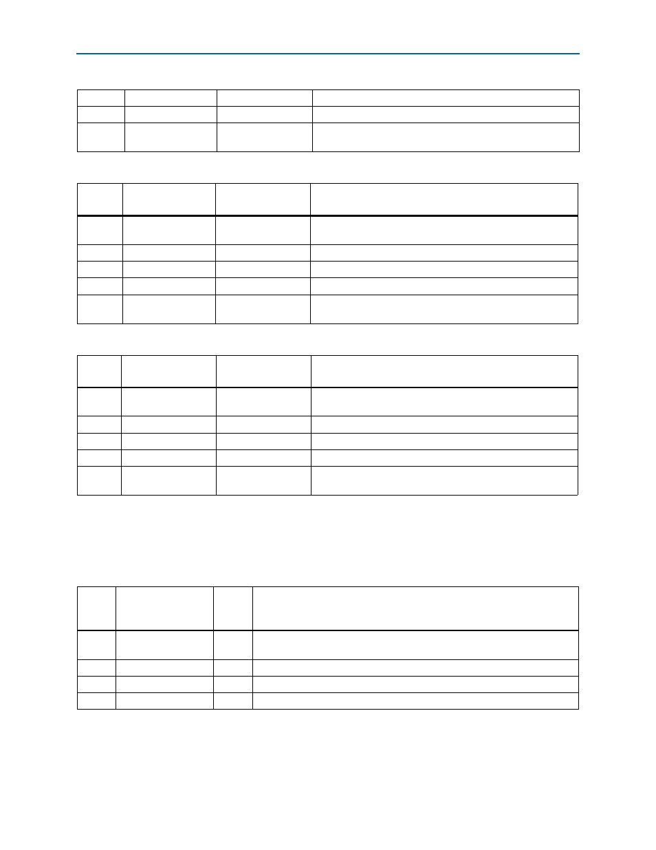
Table 15–14. Write Descriptor 0
Table 15–15. Write Descriptor 1
Offset in BFM
Shared Memory
Value
Description
DW0
0x820 1,024
Transfer length in DWORDS and control bits as described in
DW1
0x824
0
Endpoint address
DW2
0x828
0
BFM shared memory data buffer 1 upper address value
DW3
0x82c
0x2800
BFM shared memory data buffer 1 lower address value
Data
Buffer 1
0x02800
Increment by 1 from
0x2525_0001
Data content in the BFM shared memory from address: 0x02800
Table 15–16. Write Descriptor 2
Offset in BFM
Shared Memory
Value
Description
DW0
0x830 644
Transfer length in DWORDS and control bits as described in
DW1
0x834
0
Endpoint address
DW2
0x838
0
BFM shared memory data buffer 2 upper address value
DW3
0x83c
0x057A0
BFM shared memory data buffer 2 lower address value
Data
Buffer 2
0x057A0
Increment by 1 from
0x3535_0001
Data content in the BFM shared memory from address: 0x057A0
Table 15–17. DMA Control Register Setup for DMA Write
Offset in DMA
Control Register
(BAR2)
Value
Description
DW0
0x0
3
Number of descriptors and control bits as described in
DW1
0x4
0
BFM shared memory descriptor table upper address value
DW2
0x8
0x800
BFM shared memory descriptor table lower address value
DW3
0xc
2
Last valid descriptor