3 output circuit signal allocation – Yaskawa Sigma II Series DC Power Input SGMAJ User Manual
Page 168
7 Digital Operator
7.3.3 Output Circuit Signal Allocation
7-24
7.3.3 Output Circuit Signal Allocation
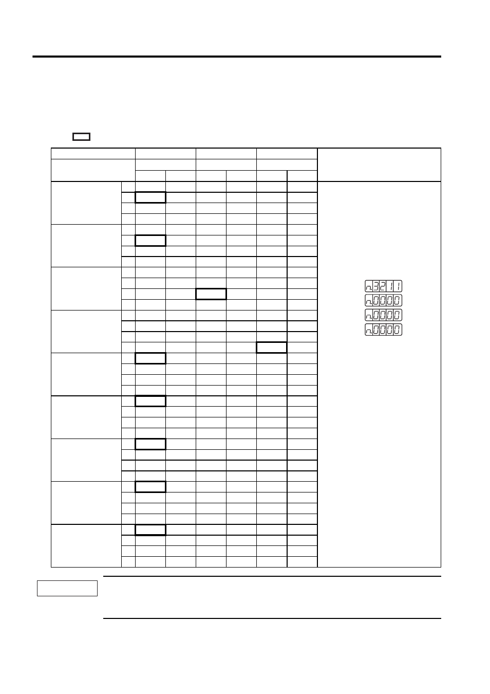
Functions can be allocated to the following sequence output signals. After having changed the parameter, turn
OFF the power and ON again to enable the parameters.
means factory setting.
1. When two or more signals are allocated to the same output circuit, a signal is output with OR logic.
2. The signals not detected are considered as “Invalid.” For example, Positioning Completion (/COIN) Sig-
nal in the SGDJ-S speed control mode is “Invalid.”
CN1 Pin No.
8/(10)
9/(10)
7/(10)
Remark
Parameter Setting
Allocation
Pn512=n.xxx
Pn512=n.xxx
Pn512=n.xxx
0
1
0
1
0
1
Positioning
Completion
(/COIN)
Pn50E.0 = n.xxx
0
Invalid
L:
Valid output signal: Low level
H:
Valid output signal: High level
Invalid:
Do not use the output signal.
Factory Setting
Note:
The output signals for Positioning
Completion Signal and Speed Coinci-
dence Detection Signal differ depend-
ing on the control method.
1
L
H
2
L
H
3
L
H
Speed Coinci-
dence Detection
(/V-CMP)
Pn50E.1 = n.xxx
0
Invalid
1
L
H
2
L
H
3
L
H
Rotation Detection
(/TGON)
Pn50E.2 = n.xxx
0
Invalid
1
L
H
2
L
H
3
L
H
Servo Ready
(/S-RDY)
Pn50E.3 = n.xxx
0
Invalid
1
L
H
2
L
H
3
L
H
Torque Limit
Detection
(/CLT)
Pn50F.0 = n.xxx
0
Invalid
1
L
H
2
L
H
3
L
H
Speed Limit
Detection
(/VLT)
Pn50F.1 = n.xxx
0
Invalid
1
L
H
2
L
H
3
L
H
Brake
(/BK)
Pn50F.2 = n.xxx
0
Invalid
1
L
H
2
L
H
3
L
H
Warning
(/WARN)
Pn50F.3 = n.xxx
0
Invalid
1
L
H
2
L
H
3
L
H
Near
(/NEAR)
Pn510.0 = n.xxx
0
Invalid
1
L
H
2
L
H
3
L
H
Pn512:
Pn510:
Pn50F:
Pn50E:
IMPORTANT