3 terminal block configuration – Yaskawa VS-626 MC5 User Manual
Page 38
3.3
Terminal Block Configuration
- 5
1.
Control circuit terminals 1 to 33 are not arranged in order of terminal numbers; they are arranged as shown
below. Be sure to wire them correctly.
21
22
23
9
10
25
26
27
33
18
19
20
11
12(G)
1
2
3
4
5
6
7
8
13
14
15
16
17
2. Do not use control circuit terminals 13 and 14 at the same time.
(The two signals will be added inside the Inverter if they are input at the same time.)
3. The maximum output current capacity of the +15 V/--15 V output from control circuit terminals 15 and
33 is 20 mA.
4. The multi-function analog output is a dedicated meter output for a frequency meter, ammeter, etc. Do not
use this output for feedback control or for any other control purpose.
Use one of the optional Analog Monitor Cards (AO-08 or AO-012) for analog outputs to the control sys-
tem.
5. Disable the stall prevention during deceleration (set constant L3-04 to 0) when using a Braking Resistor
Unit. If this user constant is not changed to disable stall prevention, the system may not stop during decel-
eration.
6. Set constant L8--01 to 1, 2 or 3 to enable protection for the internal DB resistor (model ERF) when using
an internal braking resistor. The braking resistor will not be protected unless this setting is changed to
enable protection.
7. DC reactors to improve the input power factor can be connected as an option only to Inverters for 15 kW
or less. Remove the short bar from between ¨1 and ¨2 when connecting a DC reactor.
8. There is no DC power supply input terminals for 200 V class Inverters of 30 to 75 kW and 400 V class
Inverters of 55 to 75 kW, and DC power cannot be input to these Inverters.
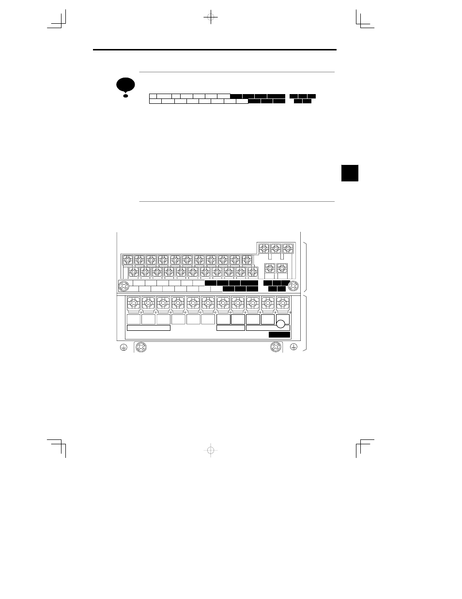
3.3
Terminal Block Configuration
The terminal block for a 200 V class Inverter with an output of 0.4 kW is shown in Figure 3.3.
Control circuit
terminals
Main circuit
terminals
10
B2
V
T2
Power input
Braking resistor
Motor output
CHARGE
1
2
3
4
5
6
7
8
21
22
23
9
11 12(G)
13
14
15
16
17
25
26
27
33
18
19
20
R
L1
S
L2
T
L3
©
¨
1
¨
2
B1
W/T3
U
T1
Fig
3.3
Terminal Arrangement
3
NOTE