Transceiver block architecture, Analog section overview, Transmitter differential i/o buffers – Altera Stratix GX Transceiver User Manual
Page 10: Receiver differential i/o buffers, Transceiver block architecture –2, Settings that support noise margin tuning
1–2
Altera Corporation
Stratix GX Transceiver User Guide
January 2005
Transceiver Block Architecture
Transceiver
Block
Architecture
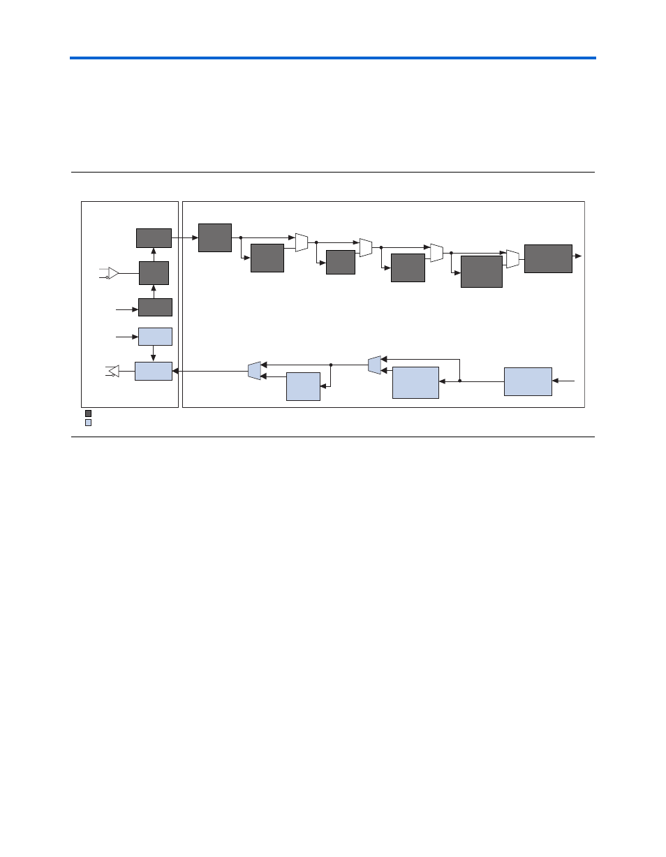
shows a block diagram of the gigabit transceiver block (GXB).
You can bypass various modules if desired. Refer to
for a description of the supported features in
each mode. You can divide the transceiver block into an analog section
and a digital section, as shown in
Figure 1–1. Block Diagram of a Stratix GX Gigabit Transceiver Block
Analog Section Overview
This section describes the various components within the analog section
of the transceiver block.
Transmitter Differential I/O Buffers
The gigabit transmitter block differential I/O buffers support the 1.5-V
PCML I/O standard, and contain features that improve system signal
integrity. These features include programmable pre-emphasis, which
helps compensate for high frequency losses, and a variety of
programmable V
OD
settings that support noise margin tuning.
Receiver Differential I/O Buffers
The gigabit transceiver block differential I/O buffers support the 1.5-V
PCML I/O standard, and contain a variety of features that improve
system signal integrity. Programmable equalization capabilities are used
to compensate for signal degradation across transmission mediums.
Deserializer
Serializer
Word
Aligner
8B/10B
Decoder
Channel
Aligner
Byte
Deserializer
8B/10B
Encoder
Phase
Compensation
FIFO Buffer
Reference
Clock
Reference
Clock
Byte
Serializer
Phase
Compensation
FIFO Buffer
Rate
Matcher
Digital Section
Analog Section
Receiver
PLL
Transmitter
PLL
Clock
Recovery
Unit
Receiver
Transmitter