Figure 5–26, Show – Altera Stratix GX Transceiver User Manual
Page 144
5–32
Altera Corporation
Stratix GX Transceiver User Guide
January 2005
XAUI Mode Clocking
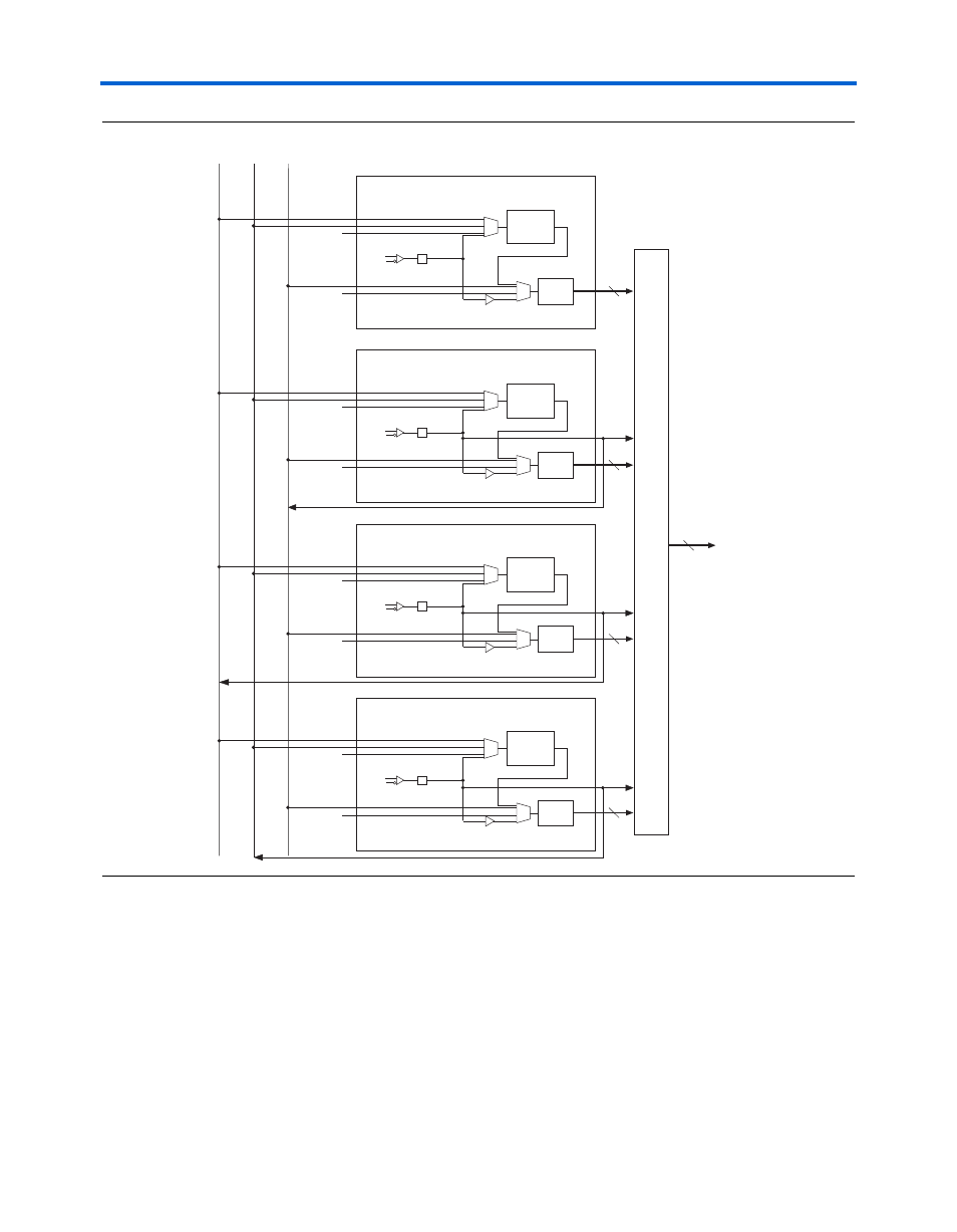
Figure 5–26. IQ Line Connections for EP1SGX25 Device
shows the transceiver routing with respect to IQ lines for the
EP1SGX40G device. This device has an extra transceiver block
(transceiver block 4), which is in the middle of the other transceiver
blocks, as shown. It is important to use this information when placing
refclkb
pins. (When placing refclkb pins, see
for information about analog reads and refclkb pin
usage constraints.)
16
IQ0
IQ1
IQ2
Transceiver Block 0
IQ0
IQ1
Global Clocks, I/O Bus, General Routin
g
Global Clocks, I/O Bus, General Routin
g
Transmitter
PLL
IQ2
/2
4
4
Receiver
PLLs
PLD Global Clocks
Transceiver Block 1
IQ0
IQ1
Global Clocks, I/O Bus, General Routin
g
Global Clocks, I/O Bus, General Routin
g
Transmitter
PLL
IQ2
/2
4
4
Receiver
PLLs
Transceiver Block 2
IQ0
IQ1
Global Clocks, I/O Bus, General Routin
g
Global Clocks, I/O Bus, General Routin
g
Transmitter
PLL
IQ2
/2
4
4
Receiver
PLLs
Transceiver Block 3
IQ0
IQ1
Global Clocks, I/O Bus, General Routin
g
Global Clocks, I/O Bus, General Routin
g
Transmitter
PLL
IQ2
/2
4
4
Receiver
PLLs
refclkb
refclkb
refclkb
refclkb