Rm in, Figure 9–12, Shows the funct – Altera Stratix GX Transceiver User Manual
Page 260
9–34
Altera Corporation
Stratix GX Transceiver User Guide
January 2005
Recommended Resets
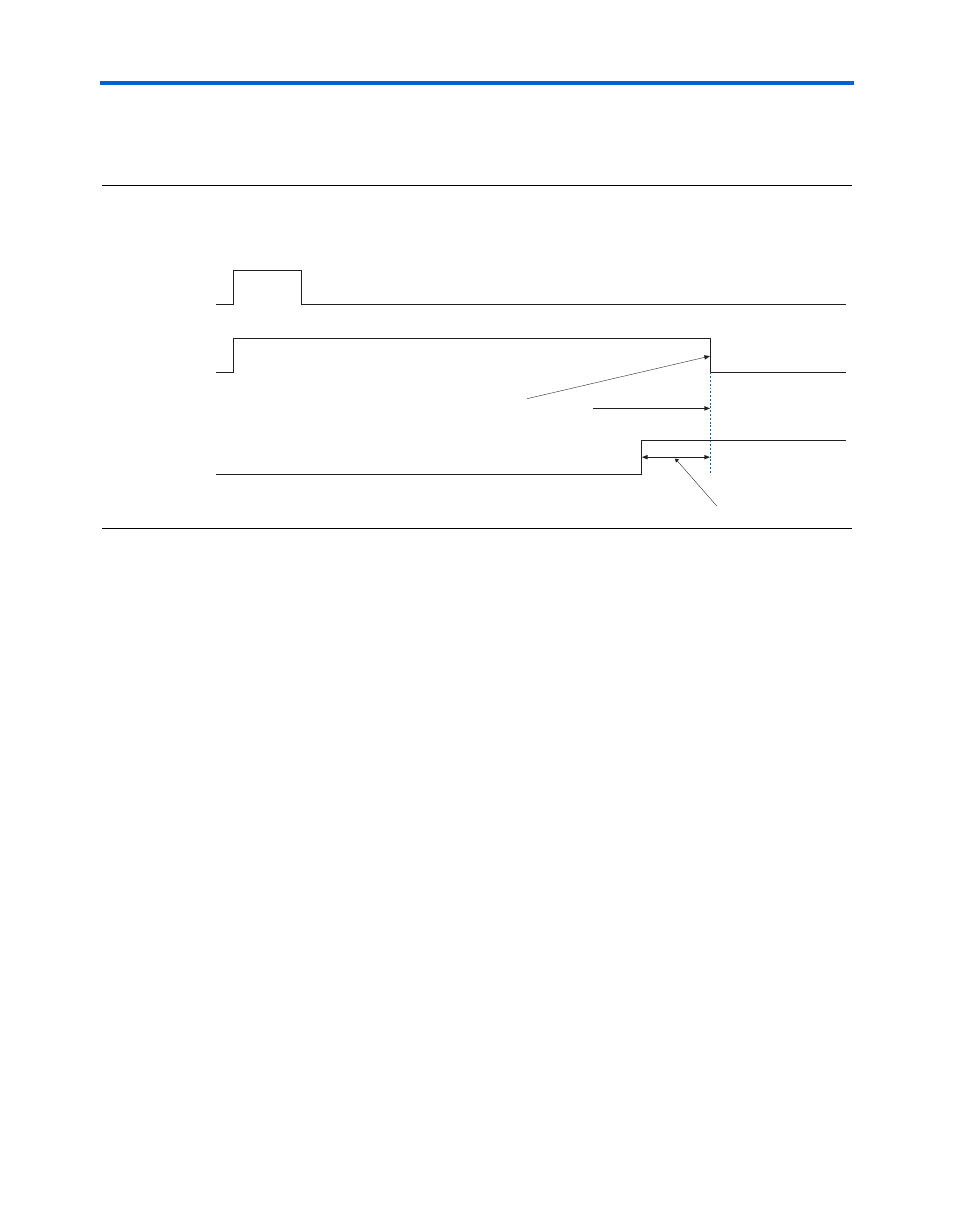
f
See the Stratix GX FPGA Family data sheet for the value of
Trx_freqlock2phaselock
.
Figure 9–12. Receiver Reset Sequence Waveform
Design Example 1
This design example shows a receive only configuration where inclk is
the transmit PLL input reference clock, the output of transmit PLL trains
receive CRU, and rx_coreclk is the receive parallel interface clock.
This design example has following constraints:
■
If your design requirements are different from the examples, use the
flow charts and waveforms for each configuration as design
guidelines.
■
The design example requires a reset controller that generates a
sync_reset
(synchronous reset) for the entire system.
■
The design example has an async_reset (a power down in GXB
terms) and digital resets for transmit and receive. All user input
digital resets must be at least four cycles long.
■
This design example does not cover all the digital reset scenarios in
a system that resets the digital logic of the GXB.
■
In this example, whenever the rx_freqlocked signal toggles the
rxdigitalreset
, the receiver’s digital circuit is reset. However,
you can make changes to the design to avoid this if, for example, you
want to debug your design without the core being reset.
■
If you plan to use REFCLKB pins in your design, see
for information about the effects of analog
resets (pll_arest, rx_analogreset).
Stable Recovered Clock
1
2
3
4
rx_analogreset
rx_digitalreset
rx_freqlocked
Output Status
Reset Signals
Trx_freqlock2phaselock