Receiver phase compensation fifo module, Xaui mode transmitter architecture, Transmitter phase compensation fifo module – Altera Stratix GX Transceiver User Manual
Page 130: Xaui mode transmitter architecture –18
5–18
Altera Corporation
Stratix GX Transceiver User Guide
January 2005
XAUI Mode Transmitter Architecture
Receiver Phase Compensation FIFO Module
The receiver phase compensation FIFO module is located at the FPGA
logic array interface in the receiver block and is four words deep. The
FIFO module compensates for the phase difference between the clock in
the FPGA and the operating clocks in the transceiver block.
In XAUI mode, the write port is clocked by the refclk from the
transmitter PLL. This clock is half the rate if the byte deserializer is used.
The read clock is clocked by coreclk (output from the transmitter PLL).
The receiver phase compensation FIFO module only accounts for phase
differences.
The receiver phase compensation FIFO module is always used and
cannot be bypassed.
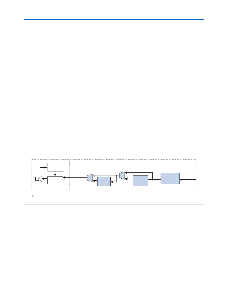
XAUI Mode
Transmitter
Architecture
diagrams the transmitter digital components in XAUI mode.
Figure 5–15. Block Diagram of Transmitter Digital Components in XAUI Mode
Transmitter Phase Compensation FIFO Module
The Transmitter Phase Compensation FIFO module is located at the
FPGA logic array interface in the transmitter block and is four words
deep. The FIFO module compensates for the phase difference between
the clock in the FPGA and the operating clocks in the transceiver block.
The read port of the phase compensation FIFO module is clocked by the
transmitter PLL clock. The write clock is clocked by tx_coreclk. You
can select the tx_coreclk as an optional transmitter input port to
Byte
Serializer
Phase
Compensation
FIFO Buffer
Serializer
8B/10B
Encoder
Transmitter
Reference
Clock
Transmitter
PLL
Analog Section
Digital Section