Receiver phase compensation fifo buffer, Gige mode transmitter architecture, Gige mode transmitter architecture –14 – Altera Stratix GX Transceiver User Manual
Page 168
6–14
Altera Corporation
Stratix GX Transceiver User Guide
January 2005
GigE Mode Transmitter Architecture
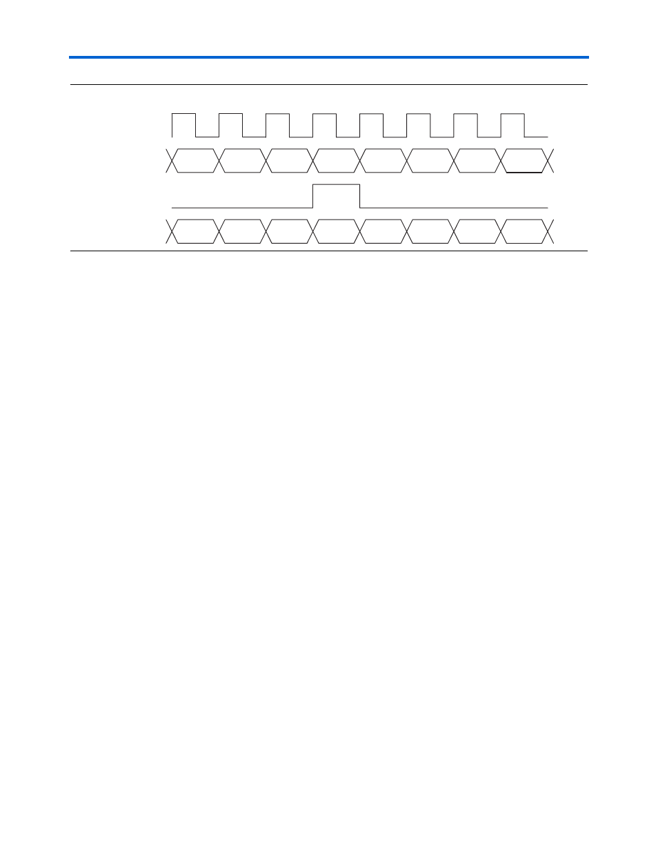
Figure 6–14. Control Code Detection
Receiver Phase Compensation FIFO Buffer
The receiver phase compensation FIFO buffer is located at the FPGA logic
array interface in the receiver block and is four words deep. This FIFO
buffer compensates for the phase difference between the clock in the
FPGA and the operating clocks in the transceiver block.
In GigE mode, the write port is clocked by the refclk from the
transmitter phase-locked loop (PLL). The read clock is clocked by
CORECLK
(output from the transmitter PLL). The receiver phase
compensation FIFO buffer can only account for phase differences and
must be derived from the recovered clock of its associated channel.
The receiver phase compensation FIFO buffer is always used, and you
cannot bypass it.
GigE Mode
Transmitter
Architecture
shows the digital components of the Stratix GX transmitter
that are active in GigE mode.
clock
rx_out[7:0]
rx_ctrldetect
83
78
BC
07
0F
00
BF
3C
D3.4
D24.3
D28.5
K28.5
D15.0
D0.0
D31.5
D28.1
Code Group