Altera Stratix GX Transceiver User Manual
Page 101
Altera Corporation
4–19
January 2005
Stratix GX Transceiver User Guide
SONET Mode
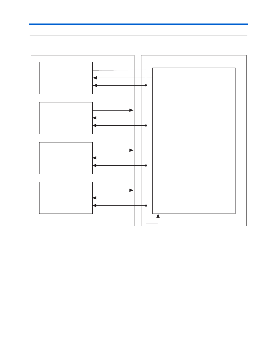
Figure 4–14. Example of a Multi-Transceiver Block FPGA to Transmitter Interface Clocking Scheme in SONET
Mode
When tx_coreclk is not enabled, the Quartus II software automatically
routes the coreclk_out signal to the write clock of the phase
compensation FIFO module via a global, regional, or fast regional
resource. In multi-transceiver block configuration, this routing might
lead to timing violations because the coreclk_out per transceiver block
cannot guarantee phase relationship. For this reason, Altera recommends
clocking the tx_coreclk with a common clock for synchronous
transmission.
Another inter-transceiver block consideration is the selection of the
dedicated refclkb pin. Stratix GX channels are arranged in banks of
four, or transceiver blocks. Each transceiver block has the ability to share
a common reference clock through the inter-transceiver (IQ) lines. The
Transceiver Block 0
Transceiver Block 1
Transceiver Block 2
Transceiver Block 3
PLD Transmit Data
Clock Domain
coreclk_out[0]
tx_in_0[15..0]
tx_coreclk[0]
coreclk_out[1]
tx_in_1[15..0]
tx_coreclk[1]
coreclk_out[2]
tx_in_2[15..0]
tx_coreclk[2]
coreclk_out[3]
tx_in_3[15..0]
tx_coreclk[3]
Altera Gigabit Transceiver Block
PLD