Altera Stratix GX Transceiver User Manual
Page 180
6–26
Altera Corporation
Stratix GX Transceiver User Guide
January 2005
GigE Mode Clocking
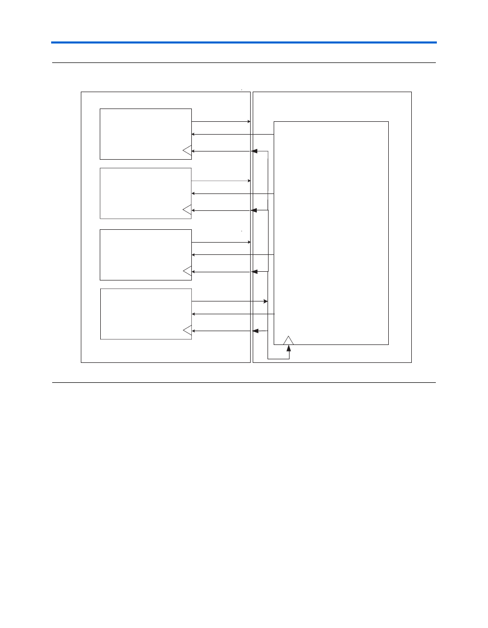
Figure 6–24. Example of a Multi-Transceiver PLD to Transmitter Interface Clocking Scheme
When TX_CORECLK is not enabled, the Quartus II software automatically
routes the signal from the CORECLK_OUT port to the write clock of the
phase compensation FIFO buffer using a global, regional, or fast regional
resource. In a multi-transceiver configuration, this routing can lead to
timing violations because the coreclk_out per transceiver block cannot
guarantee a phase relationship. Therefore, clocking the TX_CORECLK
with a common clock is recommended for synchronous transmission.
Another inter-transceiver consideration is the selection of the dedicated
REFCLKB
pin. Stratix GX channels are arranged in banks of four (called
transceiver blocks). Each transceiver block has the ability to share a
common reference clock through the inter-transceiver lines (IQ lines). The
Stratix GX logic array clock usage can be reduced by using the IQ lines.
The IQ lines are used when a REFCLKB input port from one transceiver
block or channel drives other transceiver blocks or channels. The
Quartus I software automatically determines the IQ line usage.
ALTGXB
PLD
Transceiver Block 0
Transceiver Block 1
coreclk_out[0]
tx_coreclk[0]
tx_coreclk[1]
PLD Transmit Data
Clock Domain
tx_in_0[15..0]
coreclk_out[1]
tx_coreclk[1]
tx_in_1[15..0]
Transceiver Block 2
Transceiver Block 3
coreclk_out[2]
tx_coreclk[2]
tx_in_2[15..0]
coreclk_out[3]
tx_coreclk[3]
tx_in_3[15..0]