Receiver phase compensation fifo module, Seen in, Figure 4–8 – Altera Stratix GX Transceiver User Manual
Page 92
4–10
Altera Corporation
Stratix GX Transceiver User Guide
January 2005
SONET Mode Receiver Architecture
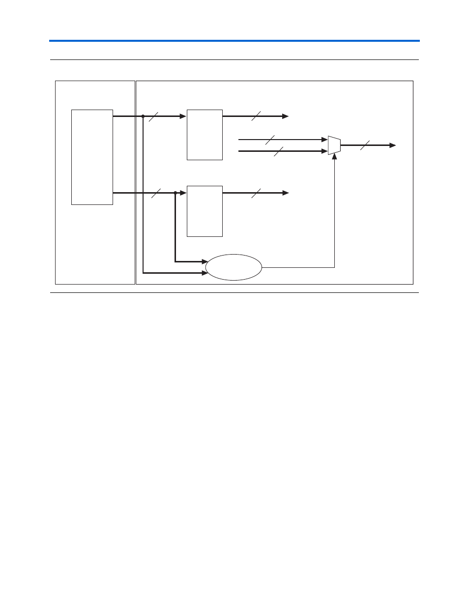
Figure 4–8. Receiver Byte Deserializer Data Recovery in Logic Array
Receiver Phase Compensation FIFO Module
The receiver phase compensation FIFO module is located at the FPGA
logic array interface in the receiver block and is four words deep. The
FIFO module compensates for the phase difference between the clock in
the FPGA and the operating clocks in the transceiver block.
In SONET mode, the write port is clocked by the recovered clock from the
CRU. The rate of this clock is reduced by half if the byte deserializer is
used. The read clock is clocked by rx_coreclk.
You can select rx_coreclk as an optional receiver input port that can
also accept a clock supply. The clock that feeds the rx_coreclk must be
derived from the rx_clkout of its associated receiver channel. The
receiver phase compensation FIFO buffer can only account for phase
differences.
In SONET mode, if you do not select the rx_clkout port, the read clock
of the receiver phase compensation FIFO module, clocked by
rx_coreclk
, is fed by rx_clkout. An FPGA global clock, regional
clock, or fast regional clock resource is required to make the connection
Gigabit Transceiver Block
Logic Array
D
Q
D
Q
rx_out[19..10]
rx_out[9..0]
Byte Boundary
Selection Logic
rx_out_post[9..0]
rx_out_post[19..10]
{rx_out[9..0], rx_out_post[19..10]}
rx_out_post[19..0]
rx_out_align[19..0]
Phase
Compensation
FIFO
Buffer
10
10
10
10
20
10
10