Gige mode inter-transceiver clocking – Altera Stratix GX Transceiver User Manual
Page 179
Altera Corporation
6–25
January 2005
Stratix GX Transceiver User Guide
GigE Mode
GigE Mode Inter-Transceiver Clocking
This section provides guidelines for using transceiver interface clocking
between the PLD logic array and transceiver channels when multiple
transceiver blocks are active. Depending on which mode is supported by
Stratix GX devices, each transceiver block has different transceiver-to-
PLD interface clocking. Different input and output clocks are available
based on the options provided by Quartus II MegaWizard built-in
functions. The number of supported channels varies based on the type of
Stratix GX device you select. Because of the various configurations of the
input and output clocks, consider the clocking schemes between
transceiver blocks carefully to avoid future problems in the design cycle.
One of the clocking interfaces to consider while designing with Stratix GX
is the transceiver-to-PLD interface. This clocking scheme can be further
classified as the PLD-to-transmitter channel and receiver channel to the
PLD.
In GigE mode, the read port of the transmitter phase compensation FIFO
buffer can either be clocked by the CORECLK_OUT or the TX_CORECLK
port. The constraint on using TX_CORECLK port is that the clock must be
frequency locked to the read port of the transmitter phase compensation
FIFO buffer. Synchronous data transfers for a multi-transceiver
configuration are accomplished with the TX_CORECLK port. The
TX_CORECLK
of multiple transceivers can be connected to a common
clock domain, either from a single CORECLK_OUT signal or from a PLD
system clock domain. This scheme is shown in
.
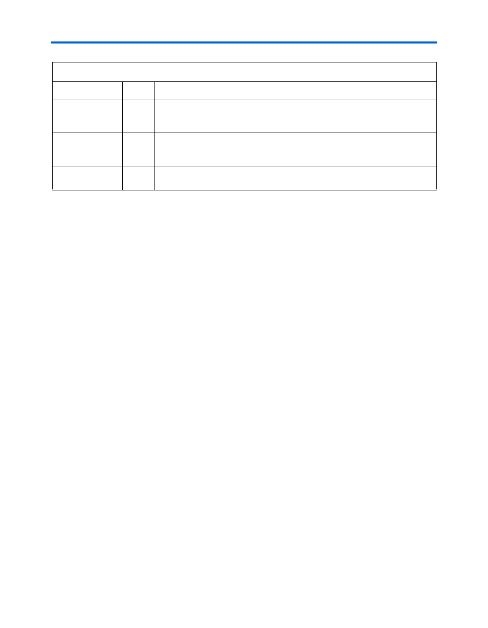
TX_CORECLK
Input
Clocks the write port of transmitter phase compensation FIFO buffer. Optional port
in Quartus II software. Must be frequency matched to
TX_PLL_CLK
. If not
available as a port, is fed by
CORECLK_OUT
through logic array routing.
RX_CORECLK
Input
Clocks the read port of receiver phase compensation FIFO buffer. Optional port in
Quartus II software. If not available as a port, is fed by
CORECLK_OUT
through
logic array routing.
CORECLK_OUT
Output
Output clock from transmitter PLL equivalent to
TX_PLL_CLK
. Available as a port
if transmitter PLL is used.
Table 6–2. Clocks in GigE Mode (Part 2 of 2)
Clock
Port
Description