Basic mode transmitter architecture, Transmitter phase compensation fifo buffer, Basic mode transmitter architecture –16 – Altera Stratix GX Transceiver User Manual
Page 62
3–16
Altera Corporation
Stratix GX Transceiver User Guide
January 2005
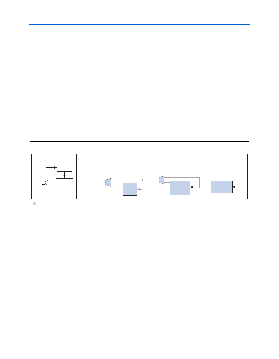
Basic Mode Transmitter Architecture
In basic mode, if the RX_CLKOUT port is not selected for use, the read
clock is clocked by RX_CORECLK, which is fed by RX_CLKOUT. An FPGA
global clock, regional clock, or fast regional clock resource is required to
make the connection for the read clock. Refer to the section
Channel Clocking” on page 3–20
or the block diagram in the MegaWizard
Plug-In Manager for more information on the clock structure in a
particular mode.
The receiver phase compensation FIFO buffer is always used and cannot
be bypassed.
Basic Mode
Transmitter
Architecture
shows the components of the transmitter block that are used
in the basic mode of operation.
Figure 3–14. Block diagram of the Transmitter Digital Components in Basic Mode
Transmitter Phase Compensation FIFO Buffer
The transmitter phase compensation FIFO buffer is located at the FPGA
logic array interface in the transmitter block and is four words deep. The
phase compensation FIFO buffer compensates for the phase difference
between the clock in the FPGA and the operating clocks in the transceiver
block.
The read port of the phase compensation FIFO module is clocked by the
transmitter PLL clock. The write clock is clocked by TX_CORECLK. You
can select the TX_CORECLK as an optional transmitter input port in which
to supply a clock. In this case, you must ensure that there is no frequency
difference between the TX_CORECLK and the Transmitter PLL clock. The
transmitter phase compensation FIFO buffer can only account for phase
differences.
Serializer
8B/10B
Encoder
Reference
Clock
Byte
Serializer
Digital Section
Analog Section
Transmitter
Phase
Compensation
FIFO Buffer
Transmitter
PLL