Altera Stratix GX Transceiver User Manual
Page 104
4–22
Altera Corporation
Stratix GX Transceiver User Guide
January 2005
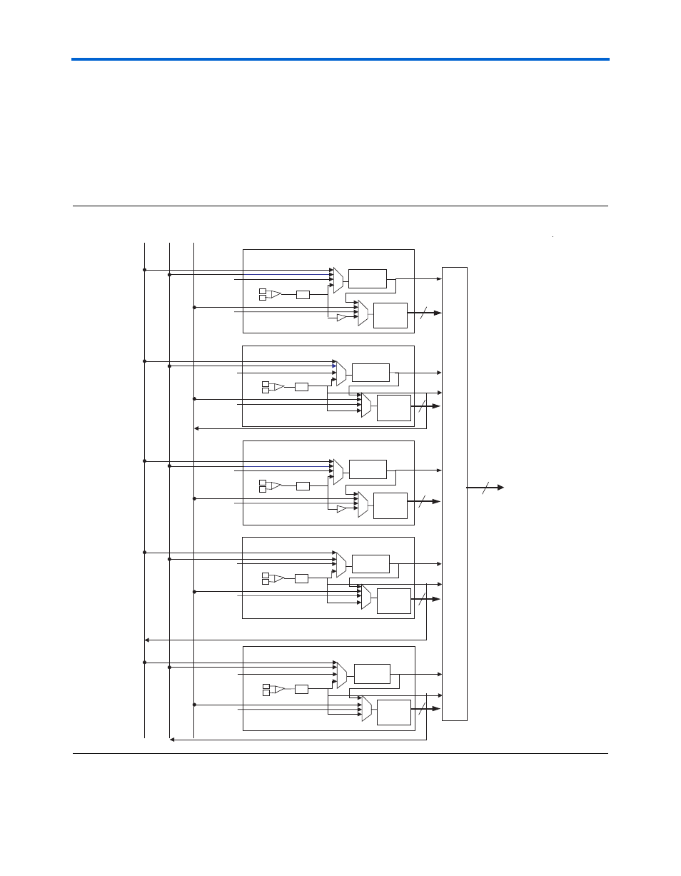
SONET Mode Clocking
shows the transceiver routing with respect to IQ lines for the
EP1SGX40G device. This device has an extra transceiver block
(transceiver block 4), in the middle of the other transceiver blocks, as
shown. Again, this information is important when determining where to
place REFCLKB pins. For example, if a REFCLKB pin is needed to feed to
a transmitter PLL using an IQ line, the pin cannot be in transceiver block 1
because IQ2 feeds only the receiver PLLs.
Figure 4–16. IQ Line Connections for EP1SGX40G Device
PLD
Global
Clocks
IQ0
IQ1
IQ2
16
Transceiver Block 2
Transmitter
PLL
IQ0
IQ1
Global Clks, I/O Bus, Gen Routing
Global Clks, I/O Bus, Gen Routing
IQ2
/2
Transceiver Block 3
Transmitter
PLL
IQ0
IQ1
Global Clks, I/O Bus, Gen Routing
Global Clks, I/O Bus, Gen Routing
IQ2
/2
Transmitter
PLL
IQ0
IQ1
Global Clks, I/O Bus, Gen Routing
Global Clks, I/O Bus, Gen Routing
IQ2
Transceiver Block 0
/2
Transceiver Block 1
Transmitter
PLL
IQ0
IQ1
Global Clks, I/O Bus, Gen Routing
Global Clks, I/O Bus, Gen Routing
IQ2
/2
Transmitter
PLL
IQ0
IQ1
Global Clks, I/O Bus, Gen Routing
Global Clks, I/O Bus, Gen Routing
IQ2
Transceiver Block 4
/2
4
4
4
4
4
refclkb
refclkb
refclkb
refclkb
refclkb
4
Receiver
PLLs
4
Receiver
PLLs
4
Receiver
PLLs
4
Receiver
PLLs
4
Receiver
PLLs