Basic mode receiver architecture, Word aligner, Basic mode receiver architecture –2 – Altera Stratix GX Transceiver User Manual
Page 48
3–2
Altera Corporation
Stratix GX Transceiver User Guide
January 2005
Basic Mode Receiver Architecture
Figure 3–1. Block Diagram of a Duplex Channel Configured in Basic Mode
Basic Mode
Receiver
Architecture
shows a block diagram of the digital components of the
receiver in basic mode.
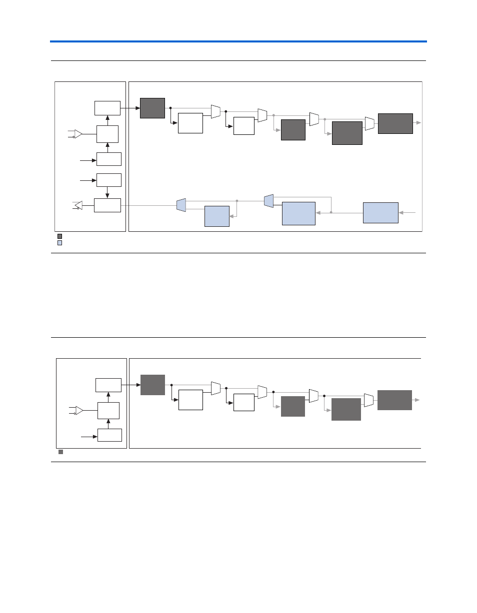
Figure 3–2. Block Diagram of the Receiver Digital Components in Basic Mode
Word Aligner
For embedded clocking schemes, the clock is recovered from the
incoming data stream based on transition density of the data. This feature
eliminates the need to factor in receiver skew margins between the clock
and data. However, with this clocking methodology, the word boundary
of the re-timed data can be altered. Stratix GX devices offer an embedded
Deserializer
Serializer
Word
Aligner
8B/10B
Decoder
Channel
Aligner
Byte
Deserializer
8B/10B
Encoder
Phase
Compensation
FIFO Buffer
Reference
Clock
Reference
Clock
Byte
Serializer
Phase
Compensation
FIFO Buffer
Rate
Matcher
Digital Section
Analog Section
Receiver
PLL
Transmitter
PLL
Clock
Recovery
Unit
Receiver
Transmitter
Deserializer
Word
Aligner
8B/10B
Decoder
Channel
Aligner
Byte
Deserializer
Phase
Compensation
FIFO Buffer
Reference
Clock
Rate
Matcher
Digital Section
Analog Section
Receiver
PLL
Clock
Recovery
Unit
Receiver