Byte serializer – Altera Stratix GX Transceiver User Manual
Page 131
Altera Corporation
5–19
January 2005
Stratix GX Transceiver User Guide
XAUI Mode
receive a clock supply. In this case, there must be no frequency difference
between the tx_coreclk and the transmitter PLL clock. The transmitter
Phase Compensation FIFO module can only account for phase
differences.
If the tx_coreclk is not selected as an optional input transmitter port,
tx_coreclk
is fed by coreclk_out. This connection occurs using the
logic array routing. As such, the software defaults to using an FPGA
global clock, regional clock, or fast regional clock resource.
The transmitter phase compensation FIFO module is always used and
cannot be bypassed. The input to this FIFO module is the data from the
FPGA logic array. If they are used, the tx_ctrlenable and
tx_forcedisparity
signals are also passed through the FIFO module
to ensure that they are synchronized with the data when they feed to the
subsequent module.
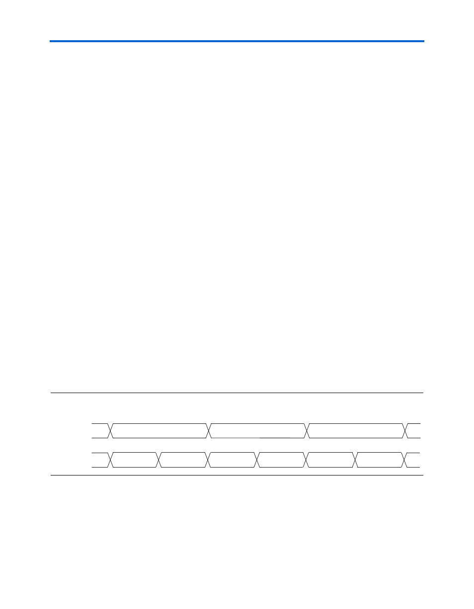
Byte Serializer
The byte serializer in the transmitter block takes a 16-bit input from the
FPGA logic array and serializes it to 8 bits. It transmits from the least
significant byte to the most significant byte. The transmitter digital reset
must always be used to reset the FIFO module pointers whenever an
unknown state is encountered, such as when the transmitter PLL loses
lock. Refer to the chapter Reset Control & Power Down for further details
on the reset sequence.
demonstrates input and output signals of the byte serializer
when serializing a 20-bit input to 10 bits. The tx_in[] signal is the input
that has already passed from the FPGA logic array through the
transmitter phase compensation FIFO module.
Figure 5–16. Transmitter Byte Serializer in 16- to 8-Bit Mode
The LSB is transmitted before the MSB in the transmitter byte serializer.
shows the order of data transmitted. For the input of D1, the
output is D1LSB and then D1MSB.
xxxxxxxx
xxxxxxxx
01101111
0001010001101111
datain[15:0]
dataout[7:0]
1100011011110001
1010101010110011
00010100
11110001
11000110
D1
D2
D3
D1 LSB
D1 MSB
D2 LSB
D2 MSB