Transmitter phase compensation fifo buffer – Altera Stratix GX Transceiver User Manual
Page 169
Altera Corporation
6–15
January 2005
Stratix GX Transceiver User Guide
GigE Mode
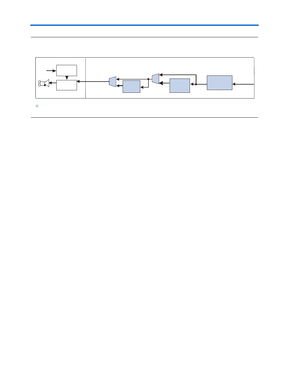
Figure 6–15. Block Diagram of Transmitter Components Configured in GigE Mode
The transmitter architecture includes:
■
Transmitter phase compensation FIFO buffer
■
GigE transmitter synchronization
■
Idle generation
■
8B/10B encoder
Transmitter Phase Compensation FIFO Buffer
The transmitter phase compensation FIFO buffer is located at the FPGA
logic array interface in the transmitter block and is four words deep. The
phase compensation FIFO buffer compensates for the phase difference
between the clock in the FPGA and the operating clocks in the transceiver
block.
The transmitter PLL output clock (refclk) clocks the read port of the
phase compensation FIFO buffer. The TX_CORECLK port clocks the write
clock. You can select the TX_CORECLK port as an optional transmitter
input port to use as a write-side clock of the FIFO buffer. Make sure that
there is no frequency difference between the TX_CORECLK port and the
transmitter PLL clock. The transmitter phase compensation FIFO only
accounts for phase differences.
If you do not select the TX_CORECLK port as an optional input transmitter
port, the CORECLK_OUT port feeds the TX_CORECLK port. This
connection occurs using the logic array routing. As a result, the software
defaults to using an FPGA global clock, regional clock, or fast regional
clock resource.
Byte
Serializer
Phase
Compensation
FIFO Buffer
Serializer
8B/10B
Encoder
Transmitter
Reference
Clock
Transmitter
PLL
Analog Section
Digital Section