Altera Stratix GX Transceiver User Manual
Page 141
Altera Corporation
5–29
January 2005
Stratix GX Transceiver User Guide
XAUI Mode
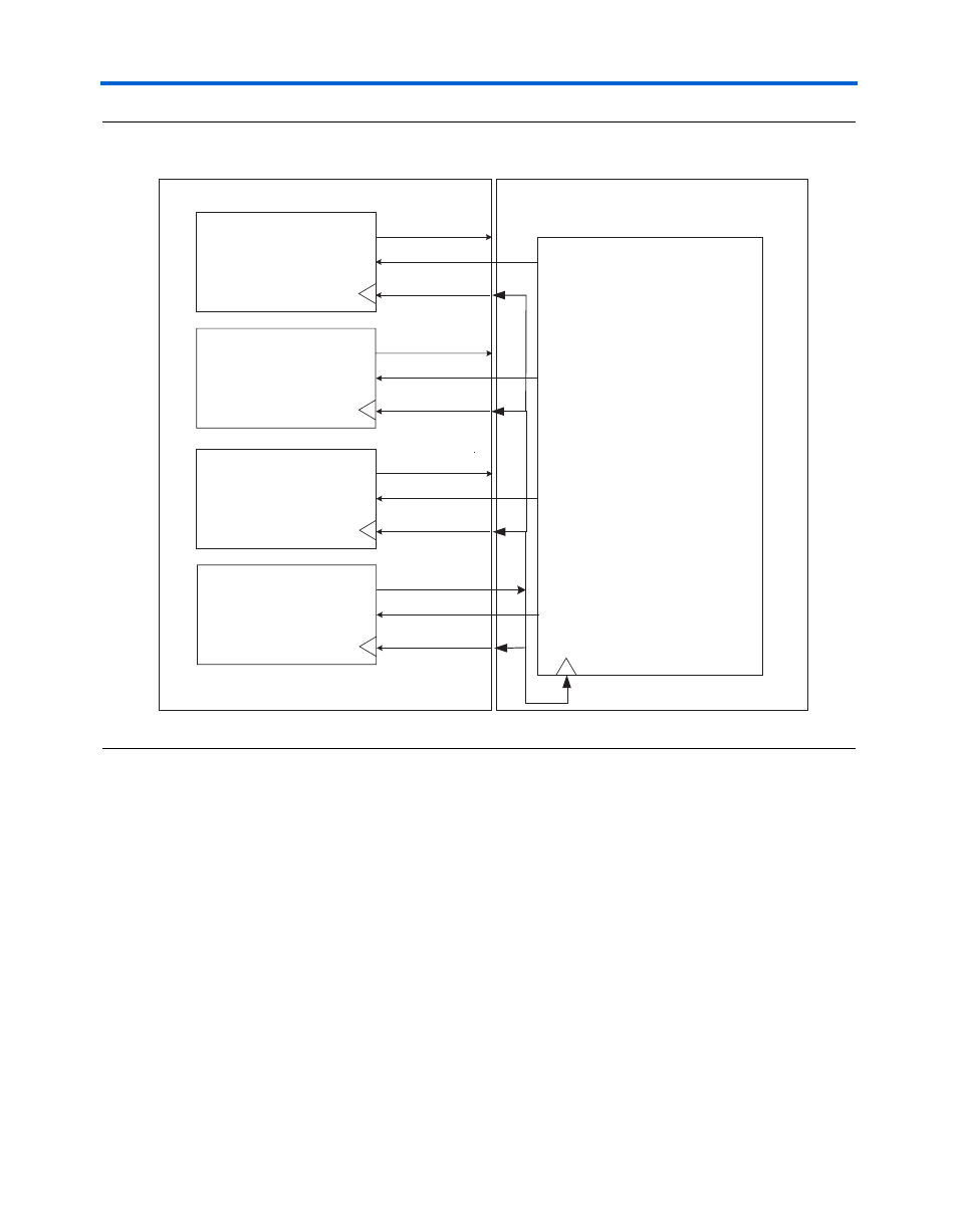
Figure 5–24. PLD to Transmit Interface Clocking Scheme in a Multi-Channel Application
At the FPGA-receive interface, there is no receive parallel interface clock
option in the MegaWizard Plug-In Manager; the default is the transmitter
PLL output clock, which is a transceiver internal clock.
Altera recommends implementing channel bonding across the
transceiver blocks used in Stratix GX devices to ensure that there is no
skew between the transceiver blocks (if each transceiver is operating, no
channel bonding is required and the data can simply go to destination
registers, as shown in
). Also, all traces in your design should
match.
ALTGXB
PLD
Transceiver Block 0
Transceiver Block 1
coreclk_out[0]
tx_coreclk[0]
tx_coreclk[1]
PLD Transmit Data
Clock Domain
tx_in_0[15..0]
coreclk_out[1]
tx_coreclk[1]
tx_in_1[15..0]
Transceiver Block 2
Transceiver Block 3
coreclk_out[2]
tx_coreclk[2]
tx_in_2[15..0]
coreclk_out[3]
tx_coreclk[3]
tx_in_3[15..0]
(GX25f)