Yaskawa MP920 User's Manual Design User Manual
Page 100
3 Basic System Operation
3.5.4 Defining Function I/O
3-26
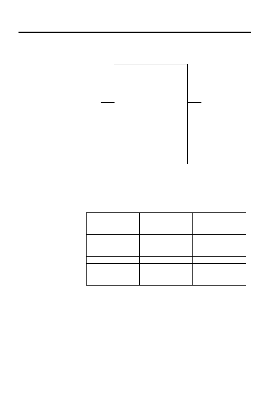
2. Fig. 3.8 shows an example of the I/O definitions of a function.
Fig. 3.8 Graphic Representation of a Function 2 (Example)
3. I/O signal addresses are automatically allocated from the highest signal on the graphic
representation. For the example given in Fig. 3.8, the allocation of each I/O register will
be as shown in Table 3.10.
Note: XW00000 and YW00000 of the X and Y registers are used for bit
data.
4. The function I/O registers shown in Fig. 3.8 are allocated automatically. The external
framework of the function is completed at this stage.
TEST
IN_01
BIT1
IN_02
BIT2
IN_03
FLT1
IN_04
INT1
IN_05
ADR
OUT_01
BIT3
OUT_02
BIT4
OUT_03
LNG1
OUT_04
INT2
Bit numeric input
Bit numeric output
Real number numeric input
Long integer numeric output
Integer numeric input
Integer numeric output
===>
===>
===>
===>
Bit numeric input
Bit numeric output
Table 3.10 Allocation of I/O Registers
Name
Data Type
I/O Register
IN_01 (BIT1)
Bit XB000000
IN_02 (BIT2)
Bit XB000001
IN_03 (FLT1)
Real number
XF00001
IN_04 (INT1)
Integer XW00003
IN_05 (ADR)
Address input
AW00000
OUT_01 (BIT3)
Bit YB000000
OUT_02 (BIT4)
Bit YB000001
OUT_03 (LNG1)
Double-length integer
YL00001
OUT_04 (INT2)
Integer YW00003