Connector pin layout (cn1 to cn4) – Yaskawa MP920 Motion Module User Manual
Page 149
Advertising
5.1 SVA-01A Module
5-7
5
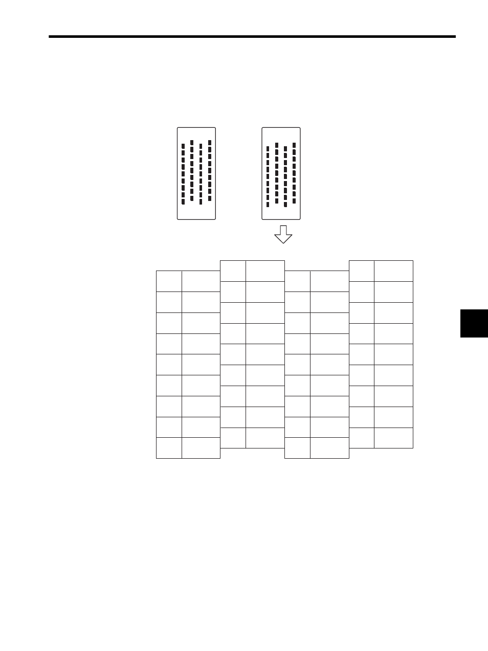
Connector Pin Layout (CN1 to CN4)
The pin layout of the CN1 to CN4 connectors are shown below.
Note: Although the connector orientation differs with each connector CN1
to CN4, the pin layout is the same for all connectors.
35
36
17
18
19
20
1
2
35
36
17
18
19
20
1
2
CN1/CN2 36-pin Connector
Pin Layout on Wiring Side
CN3/CN4 36-pin Connector
2
NREF
4
PAL
6
PCL (5V)
8
−
10
0V (24V)
12
PCON
14
OTF
16
+24V
18
BRK
1
3
5
7
9
11
13
15
17
SG
PA
PC (5V)
SG
−
0V (24V)
OTR
−
SV ALM
20
22
24
26
28
30
32
34
36
SEN (5V)
BAT
PBL
−
0V (24V)
ALM RST
SEN
(24V)
+24V
−
19
21
23
25
27
29
31
33
35
SG
0BAT
PB
SG
−
0V (24V)
SV ON
−
SRDY
Advertising
See also other documents in the category Yaskawa Equipment:
- Tag Generator (30 pages)
- MP3300iec (82 pages)
- 1000 Hz High Frequency (18 pages)
- 1000 Series (7 pages)
- PS-A10LB (39 pages)
- iQpump Micro User Manual (300 pages)
- 1000 Series Drive Option - Digital Input (30 pages)
- 1000 Series Drive Option - CANopen (39 pages)
- 1000 Series Drive Option - Analog Monitor (27 pages)
- 1000 Series Drive Option - CANopen Technical Manual (37 pages)
- 1000 Series Drive Option - CC-Link (38 pages)
- 1000 Series Drive Option - CC-Link Technical Manual (36 pages)
- 1000 Series Drive Option - DeviceNet (37 pages)
- 1000 Series Drive Option - DeviceNet Technical Manual (81 pages)
- 1000 Series Drive Option - MECHATROLINK-II (32 pages)
- 1000 Series Drive Option - Digital Output (31 pages)
- 1000 Series Drive Option - MECHATROLINK-II Technical Manual (41 pages)
- 1000 Series Drive Option - Profibus-DP (35 pages)
- AC Drive 1000-Series Option PG-RT3 Motor (36 pages)
- Z1000U HVAC MATRIX Drive Quick Start (378 pages)
- 1000 Series Operator Mounting Kit NEMA Type 4X (20 pages)
- 1000 Series Drive Option - Profibus-DP Technical Manual (44 pages)
- CopyUnitManager (38 pages)
- 1000 Series Option - JVOP-182 Remote LED (58 pages)
- 1000 Series Option - PG-X3 Line Driver (31 pages)
- SI-EN3 Technical Manual (68 pages)
- JVOP-181 (22 pages)
- JVOP-181 USB Copy Unit (2 pages)
- SI-EN3 (54 pages)
- SI-ET3 (49 pages)
- MECHATROLINK-III (35 pages)
- EtherNet/IP (50 pages)
- SI-EM3 (51 pages)
- 1000-Series Option PG-E3 Motor Encoder Feedback (33 pages)
- 1000-Series Option SI-EP3 PROFINET (56 pages)
- PROFINET (62 pages)
- AC Drive 1000-Series Option PG-RT3 Motor (45 pages)
- SI-EP3 PROFINET Technical Manual (53 pages)
- A1000 Drive Option - BACnet MS/TP (48 pages)
- 120 Series I/O Modules (308 pages)
- A1000 12-Pulse (92 pages)
- A1000 Drive Software Technical Manual (16 pages)
- A1000 Quick Start (2 pages)
- JUNMA Series AC SERVOMOTOR (1 page)
- A1000 Option DI-101 120 Vac Digital Input Option (24 pages)